MITSUMI
System Reset (with battery back-up) MM1025, 1174
System Reset (with battery back-up)
Monolithic IC MM1025, 1174
Outline
These ICs were developed for D-RAM and dummy S-RAM battery back-up. D-RAM and dummy S-RAM
power supplies differ from that of S-RAMs because 5V or 3.3V of power supply is required even during
battery back-up. Therefore, these ICs provide voltage from a stable power supply during both normal
operation and back-up. Also, the internal stable power supply switches automatically to battery back-up if the
main power supply voltage goes down for any reason.
Features
1. Battery back-up
MM1025
Current consumption
600µA typ.
Input/output voltage difference I
L
=40mA
0.25V typ.
Output current
40mA max.
MM1174
Current consumption
300µA typ.
Input/output voltage difference I
L
=40mA
0.13V typ.
Output current
40mA max.
2. Normal operation
MM1025
Input/output voltage difference
I
L
=80mA (built-in transistor)
0.29V typ.
Output current
V
CC
=6V
80mA typ.
External transistor drive current V
CC
= 6V
15mA typ.
Current consumption
900µA max.
MM1174 (for external transistor)
Input/output voltage difference
I
L
=200mA
0.13V typ.
Output current
Depends on external transistor
External transistor drive current (no built-in TR) V
CC
=3.6V
10mA typ.
Current consumption
500µA max.
3. Switching voltage from V
CC
to Battery V
CC
=High Low
MM1025
4.9V typ.
MM1174
3.25V typ.
4. V
CC
-Battery forced switching and detection voltage adjustment possible
Package
SOP-8A
Applications
1. Memory cards (D-RAM cards, other)
2. PCs, word processors and other equipment with D-RAMs
3. Fax machines, photocopiers and other office equipment with D-RAMs

MITSUMI
System Reset (with battery back-up) MM1025, 1174
Characteristics
(MM1025 series)
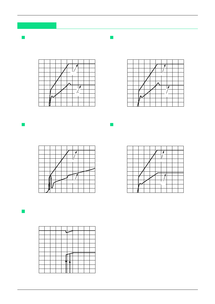
Output voltage and current consumption
for V
CC
voltage supply
I
B
ATT
(mA)
1.000
1000
0000
0000
/div
10.00
V
BATT
1.000/div (V)
.0000
5.000
.5000
/div
(V)
V
OUT
(R
L
=120
)
V
OUT
I
CC
Output voltage and current consumption for
battery voltage supply
I
BATT
(mA)
100.0
10.00
.0000
.0000
/div
V
BATT
1.000/div (V)
.0000
5.000
.5000
/div
(R
L
=120
)
(V)
V
OUT
10.00
V
OUT
I
CC
Output voltage and current consumption
for V
CC
voltage supply
10.00
I
CC
(mA)
2.000
2000
.0000
.0000
/div
V
CC
1.000/div (V)
.0000
5.000
.5000
/div
(RL=
)
(V)
V
OUT
V
OUT
I
CC
Output voltage and current consumption for
battery voltage supply
I
CC
(mA)
100.0
10.00
.0000
/div
10.00
.0000
V
BATT
1.000/div (V)
(R
L
=
)
.0000
5.000
.5000
/div
(V)
V
OUT
V
OUT
I
CC
Power supply switching voltage
6.000
V
OUT
(V)
5.000
.5000
.0000
4.0000
/div
V
CC
.2000/div (V)
.0000
100.0
10.00
/div
(mA)
I
CC
(Ta = ambient temperature)

MITSUMI
System Reset (with battery back-up) MM1025, 1174
5.0
4.8
4.6
0
500
1000
V
CC
=6.0V
V
BATT
=0V
IL (mA)
Output voltage (V)
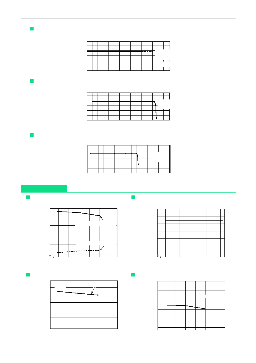
External Tr 2SA1020Y
V
CC
output current (external power transistor)
20
0
40
60
70
4.6
4.8
5.0
IL (mA)
V
CC
=0V
V
BATT
=6.0V
Output voltage (V)
V
BATT
output current
0
4.6
4.8
5.0
50
100
IL (mA)
V
CC
=6.0V
V
BATT
=0V
Output voltage (V)
(No external power transistor)
V
CC
output current (no external power transistor)
Characteristics
(MM1174 series)
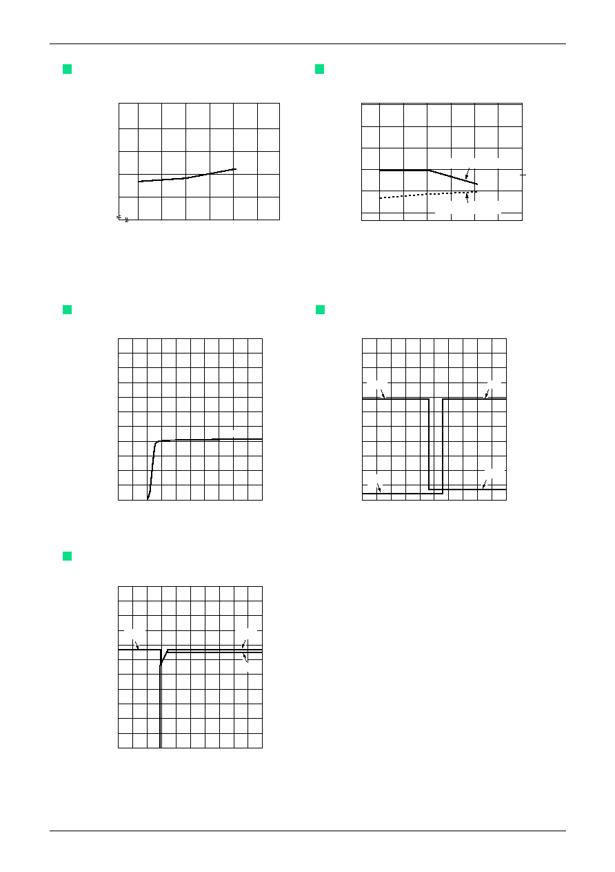
Current consumption 1-2 temperatures
Current consumption 2
-25
0
25
50
75
500
450
400
350
300
Current consumption (
µ
A)
Temperature (
∞
C)
Current consumption 1
Input/output voltage difference 1
temperature (external transistor 2SA1020)
50
100
150
200
250
I
OUT
(mA)
3.0
2.8
2.6
2.4
2.2
2.0
Output voltage (V)
Input/output voltage difference 2 temperature
2.87V
2.85V
2.80V
I
L
=-20mA
3.0
2.8
2.6
-25
0
25
50
75
Output voltage (V)
Temperature (
∞
C)
Output voltage-Temperature
V
OUT
=3mA
3.3
3.2
3.1
-25
0
25
50
75
Output voltage (V)
Temperature (
∞
C)


