 | –≠–ª–µ–∫—Ç—Ä–æ–Ω–Ω—ã–π –∫–æ–º–ø–æ–Ω–µ–Ω—Ç: MM1027NV | –°–∫–∞—á–∞—Ç—å:  PDF PDF  ZIP ZIP |

MITSUMI
System Reset (with battery back-up) MM1027, 1081
System Reset (with battery back-up)
Monolithic IC MM1027, 1081
Outline
These ICs were developed for STATIC-RAM (S-RAM) battery back-up, and have built-in switching circuit for
main power supply and battery, back-up timing circuit and battery checker.
Power ON/OFF and momentary power interruptions can damage S-RAM data on equipment that contains an
S-RAM. These ICs switch the S-RAM to back-up mode (CS signal makes S-RAM CE pin low and CE
-
--------------------------------------------------
pin high)
when power supply voltage goes below a set voltage (detection voltage 4.2V typ., variable), preventing
damage to data. Further, when power supply voltage drops, these ICs switch from main power supply to
battery back-up (switching voltage 3.3V typ.). Then, when power supply voltage rises, they first switch the S-
RAM from battery back-up state to main power supply (switching voltage 3.3V typ.), and from back-up mode
to normal mode (CS signal makes S-RAM CE pin high and CE
-
-------------------------------------------------
pin low). These signal processes provide
reliable protection against data damage. The CS signal also can absorb power supply chattering and
roughness through the external capacitor.
There is a built-in battery checker to monitor the back-up battery voltage, and this circuit is turned ON/OFF by
the control pin.
Features
1. Battery back-up
1. Low IC current consumption (loss current)
0.3µA typ.
2. Drop voltage inside IC (input/output voltage difference)
I
O
=10µA
0.2V typ.
3. Reverse current (reverse leak current)
0.1µA max.
2. Normal operation
MM1027
Drop voltage inside IC (input/output voltage difference)
I
O
=70mA
0.2V typ.
Output voltage
V
CC
=5V
I
O
=10mA
4.8V typ.
Current consumption
D.CONT OPEN
3.0mA max.
External transistor drive current
25mA typ.
MM1081
Drop voltage inside IC (input/output voltage difference)
I
O
=120mA
0.25V typ.
Output voltage
V
CC
=5V
I
O
=120mA
4.75V typ.
Current consumption
350µA max.
External transistor drive current (for output current increase)
25mA typ.
TC source current
3.0µA typ.
3. Battery-Vcc switching voltage
3.3V typ.
4. Detection voltage (CS, CS
------------------------------------------------
) variable
4.2V typ.
5. Battery checker 1
X type
2.70V typ.
N type
2.50V typ.
6. Battery checker 2
X type
2.55V typ.
N type
2.35V typ.
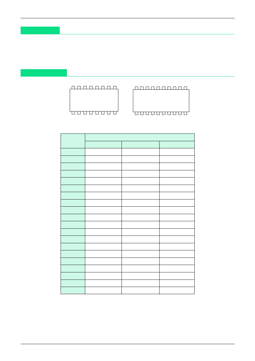
Package
TSOP-20A (MM1027XV, MM1027NV, MM1081XV)
SOP-16A (MM1027XF, MM1027NF)
DIP-16A (MM1027XD)
MITSUMI
System Reset (with battery back-up) MM1027, 1081
Applications
1. IC memory cards (RAM cards)
2. PCs, word processors
3. Fax machines, photocopiers, other office equipment
4. Other equipment with S-RAMs (equipment requiring back-up)
Pin Assignment
SOP-16A/DIP-16A
1
3
7
6
2
4 5
8
16
13
11
15 14
12
9
10
TSOP-20A
1
3
6
8
2
4 5
7
9 10
20
16
13
19
17
15 14
12
18
11
Function
Pin no.
TSOP-20A
SOP-16A
DIP-16A
1
GND
GND
GND
2
ADJ.
NC
NC
3
NC
ADJ.
ADJ.
4
TC
TC
T
C
5
NC
CS
CS
6
CS
NC
NC
7
NC
CS
-
--------------------------------------------------
CS
-
--------------------------------------------------
8
CS
-
--------------------------------------------------
DET.CONT
DET.CONT
9
NC
Bat.DET1
Bat.DET1
10
DET.CONT
NC
NC
11
Bat.DET1
Bat.DET2
Bat.DET2
12
NC
Battery
Battery
13
Bat.DET2
V
OUT
V
OUT
14
NC
External drive
External drive
15
Battery
NC
NC
16
NC
V
CC
V
CC
17
V
OUT
18
NC
19
External drive
20
V
CC
MITSUMI
System Reset (with battery back-up) MM1027, 1081
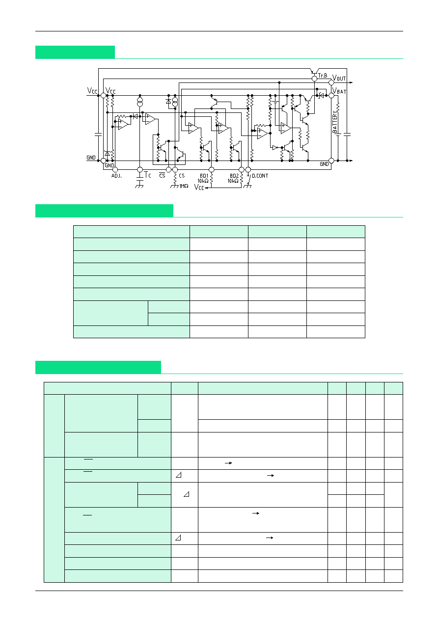
Block Diagram
Absolute Maximum Ratings
(Ta=25
∞C
)
Item
Symbol
Rating
Units
Storage temperature
T
STG
-40~+125
∞
C
Operating temperature
T
OPR
-20~+70
∞
C
Power supply voltage
V
CC
max.
7
V
Operating voltage
V
CCOP
7
V
Allowable loss
Pd
300
mW
Output current
MM1027
I
O
1
90
mA
MM1081
I
O
1
120
mA
Output current
I
O
2
200
µA
Electrical Characteristics
(Except where noted otherwise, Ta=25∞C, V
CC
=5V, V
BAT
=3V)
Item
Symbol Measurement
conditions
Min. Typ. Max. Units
Consumption
MM1027
V
CC
=5V, V
BAT
=3V, I
O
=0mA
0.9
1.7
3.0
mA
current 1
I
CC
1
D.CONT pin : OPEN
MM1081
V
CC
=5V, V
BAT
=3V, I
O
=0mA
150
210
350
µA
Consumption
MM1027
I
CC
2
V
CC
=5V, V
BAT
=3V, I
O
=0mA
1.2
2.2
3.5
mA
current 2
D.CONT pin : GND
CS, CS detection voltage 1
V
S
1
V
CC
=H L, V
BAT
=3V, ADJ pin : OPEN
4.05 4.20 4.35
V
CS, CS hysteresis voltage 1
V
S
1
V
CC
=L H
0.05 0.10 0.20
V
Detection voltage
MM1027
V
S
/ T
±0.08
%/
∞
C
temperature characteristic MM1081
±0.06
CS, CS detection voltage 2
V
S
2
V
CC
=H L, V
BAT
=3V
ADJ pin : 12k
PULL UP (to V
CC
)
3.25 3.50 3.75
V
CS, CS hysteresis voltage 2
V
S
2
V
CC
=L H
0.05 0.10 0.20
V
CS output voltage L
V
CSL
V
CC
=3V, I
CS
=3µA
0.05 0.10
V
CS output voltage H
V
CSH
V
CC
=5V, I
CS
=-3µA
4.85 4.95
V
CS source current
I
CSH
V
CC
=5V, V
CS
=4.6V current measured
8
15
µA
Note : I
O
1 expresses V
CC
output current value, and I
O
2 expresses V
BATT
output current value.
All
circuits
CS
∑
CS
---------------------------------
circuit
unit
MITSUMI
System Reset (with battery back-up) MM1027, 1081
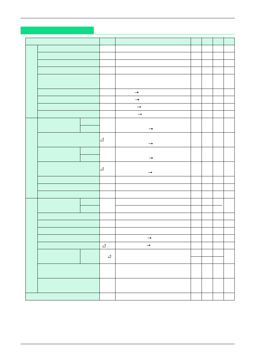
Electrical Characteristics
(Except where noted otherwise, Ta=25∞C, V
CC
=5V, V
BAT
=3V)
Item
Symbol Measurement
conditions
Min. Typ. Max. Units
CS sync current
I
CSL
V
CC
=3.5, V
CS
=0.4V Current measured
0.5
2.0
-
mA
CS
-
----------------------------------------------------
output voltage L
V
CC
=5V, I
CS
=3µA
-
0.10 0.25
V
CS
-
----------------------------------------------------
output voltage H
V
CC
=4V, V
OUT
-V
CSH
, I
CS
=-3µA
-
0.14 0.40
V
CS
-
----------------------------------------------------
sync current
V
CC
=5V, V
CS
=0.4V Current measured
0.3
1.0
-
mA
Operation limit voltage L
V
OPL
Minimum power supply voltage at which
-
2.0
2.4
V
CS pin can hold low level V
CS
<
= 0.4V
ON delay time 1
t
PLH
1
V
CC
=L H, TC : OPEN, C1=47pF
-
30
-
µS
OFF delay time 1
t
PHL
1
V
CC
=H L, TC : OPEN, C1=47pF
-
2.0
5
µS
ON delay time 2
t
PLH
2
V
CC
=L H, TC : 1nF, C1=47pF
-
0.8
-
mS
OFF delay time 2
t
PHL
2
V
CC
=H L, TC : 1nF, C1=47pF
-
2.0
10
µS
BATT
MM1027X
VBD1
V
CC
=5V, R1=10k
PULL UP
2.60 2.70 2.80
V
detection voltage 1 MM1081N
V
BAT
=H L (to V
CC
)
BATT hysteresis voltage 1
VBD1
V
CC
=5V, R1=10k
PULL UP
0.05 0.10 0.20
V
V
BAT
=L H(to V
CC
)
BATT
MM1027X
VBD2
V
CC
=5V, R2=10k
PULL UP
2.45 2.55 2.65
V
detection voltage 2 MM1081N
V
BAT
=H L (to V
CC
)
BATT hysteresis voltage 2
VBD2
V
CC
=5V, R2=10k
PULL UP
0.05 0.10 0.20
V
V
BAT
=L H (to V
CC
)
BD output voltage L
VBDL
V
CC
=5V, V
BAT
=0V
-
0.2
0.4
V
BD output sink current
IBDSNK
V
CC
=5V, V
BAT
=0V, VBD=4V
1.0
3.0
-
mA
Leakage current
IBDH
V
CC
=5V, V
BAT
=3V, VBD=5V
-
-
0.2
µA
I/O voltage
MM1027
V
SAT
1
V
CC
=5V, I
O
=70mA
-
0.2
0.3
V
difference 1
MM1081
V
CC
=5V, I
O
=120mA
-
0.25
0.4
I/O voltage difference 2
V
SAT
2
V
BAT
=3V, I
O
=10µA
-
0.2
0.3
V
I/O voltage difference 3
V
SAT
3
V
BAT
=3V, I
O
=100µA
-
0.3
0.4
V
External transistor driving current
I
BUD
V
CC
=5V, V (T
B
) =4.5V
16
25
-
mA
Power supply switching voltage
V
BB
V
CC
=H L, V
BAT
=3V
3.15 3.30 3.45
V
Hysteresis voltage
V
BB
V
CC
=L H, V
BAT
=3V
0.05 0.10 0.20
V
Switching voltage
MM1027
V
BB
/ T
-
-
±0.08
%/
∞
C
temperature characteristic MM1081
±0.06
Loss current
I
LOS
V
CC
=0V, V
BAT
=3V, I
O
=0µA
-
-
0.3
µA
D.CONT pin : GND
Reverse current
I
OREV
V
CC
=0V, V
BAT
=3V, I
O
=0µA
-
-
0.1
µA
D.CONT pin : OPEN
TC source current
I
TCSCE
V
CC
=5V, V
TC
=0V
2.0
3.0
5.0
µA
CS
-
----------------------------------------------------
∑
CS
circuit
unit
BD
circuit
unit
Backup
circuit
unit
V
CSL
-
-------------------------------------------------------------------
V
CSH
-
-------------------------------------------------
I
CSL
-
--------------------------------------------------------------
MITSUMI
System Reset (with battery back-up) MM1027, 1081
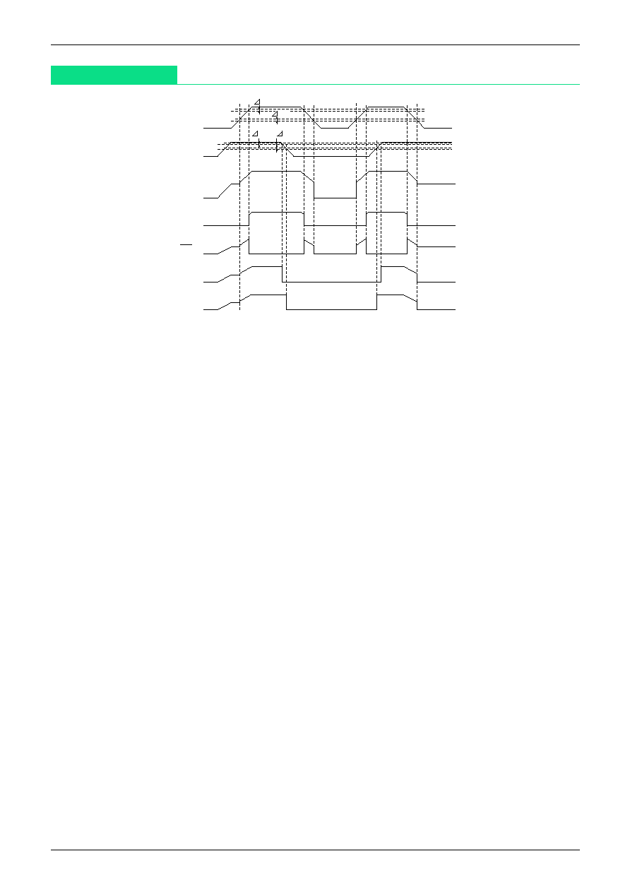
Timing Chart
V
CC
V
BATT
V
OUT
CS
V
BD1
V
BD2
CS
V
S
V
BB
V
BD2
V
BD1
V
S1
V
BB
V
BD2
V
BD1

MITSUMI
System Reset (with battery back-up) MM1027, 1081
Application Circuits
(Example : MM1027XV)
MITSUMI
System Reset (with battery back-up) MM1027, 1081
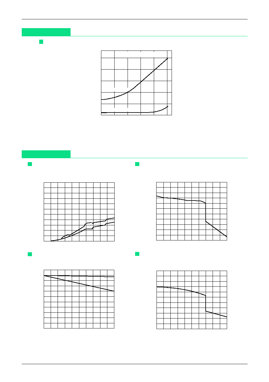
Characteristics
(MM1027X)
CS pin ON delay time V
S
. Capacitance
ON delay time
100m
10m
1m
100
µ
10
µ
1
µ
0.1
µ
0.01
µ
0.001
µ
100p
10p
1p
Delay time (S)
Capacitance (F)
OFF delay time
Vs. Capacitance
ON delay time
OFF delay time
Note : CS and CS
-
----------------------------------------------------------
output waveforms may be disturbed if delay time is more than 10mS.
Characteristics
(MM1027 series)
Current consumption
I
(mA)
5.000
.5000
/div
.0000
.0000
5.000
VI .5000/div (V)
CCONT
GND
CCONT
OPEN
Loss current during back-up
IB
(
µ
A)
2.400
0
.6000
/div
-3.600
.0000
V
BAT
=3V, I
O
=0
µ
A
5.000
V
I
.5000/div (V)
Output voltage 1
5.000
.5000
/div
.0000
.0000
V
O
(V)
-80.00
4.000
I
O
.8000/div (mA)
/div
.1000
V
OUT
V
CC
5.000
V
BAT
=3V
Shot key barrier diode reverse current
IB (
µ
A)
2.700
0
.9000
-6.300
.0000
/div
V
I
.5000/div (V)
5.000
V
BAT
=0

MITSUMI
System Reset (with battery back-up) MM1027, 1081
Output voltage 2 3
3.000
V
O
(V)
.1000
2.000
.0000
/div
-100.0
I
O
10.00/div (V)
V
CC
=0V
I
CS
-V
CS
1
I
CS
(mA)
-20.00
2.000
.0000
.0000
/div
5.000
V
CS
.5000/div (V)
CS pin
Sink current
V
CC
=4.5V
V
CS
=Variable
I
CS
-V
CS
2
I
CS
(mA)
-5.000
5.000
.0000
.0000
/div
3.500
V
CS
.3500/div (V)
CS pin
Sink current
V
CC
=3.5V
V
CS
=Variable
I
CS
-V
CS
I
CS
(mA)
5.000
.5000
0000
000
/div
5.000
V
CS
.5000/div (V)
V
CC
=5V
V
CS
=Variable
1. Connecting a resistor between ADJ pin and Vcc pin
(effective only when lowering detection voltage)
Calculated min. and max. values take
into account resistance, etc. variance
inside the IC.
Refer to Figure 1
MITSUMI
System Reset (with battery back-up) MM1027, 1081
ON delay time-Temperature
PPM
800
750
700
-770
PPM/
∞
C
-706
PPM/
∞
C
-25
0
25
50
75
100
125
Tc pin
(C
T
=1000PF
±
60PPM/
∞
C)
Delay time
Ambient temperature (
∞
C)
CS detection voltage adjustment (ADJ pin)
4.0
3.0
2.0
10
100
max.
typ.
min.
Detection voltage (V)
Resistor R1 (k
)
CS detection voltage
How to Adjust Detection Voltage Vs1
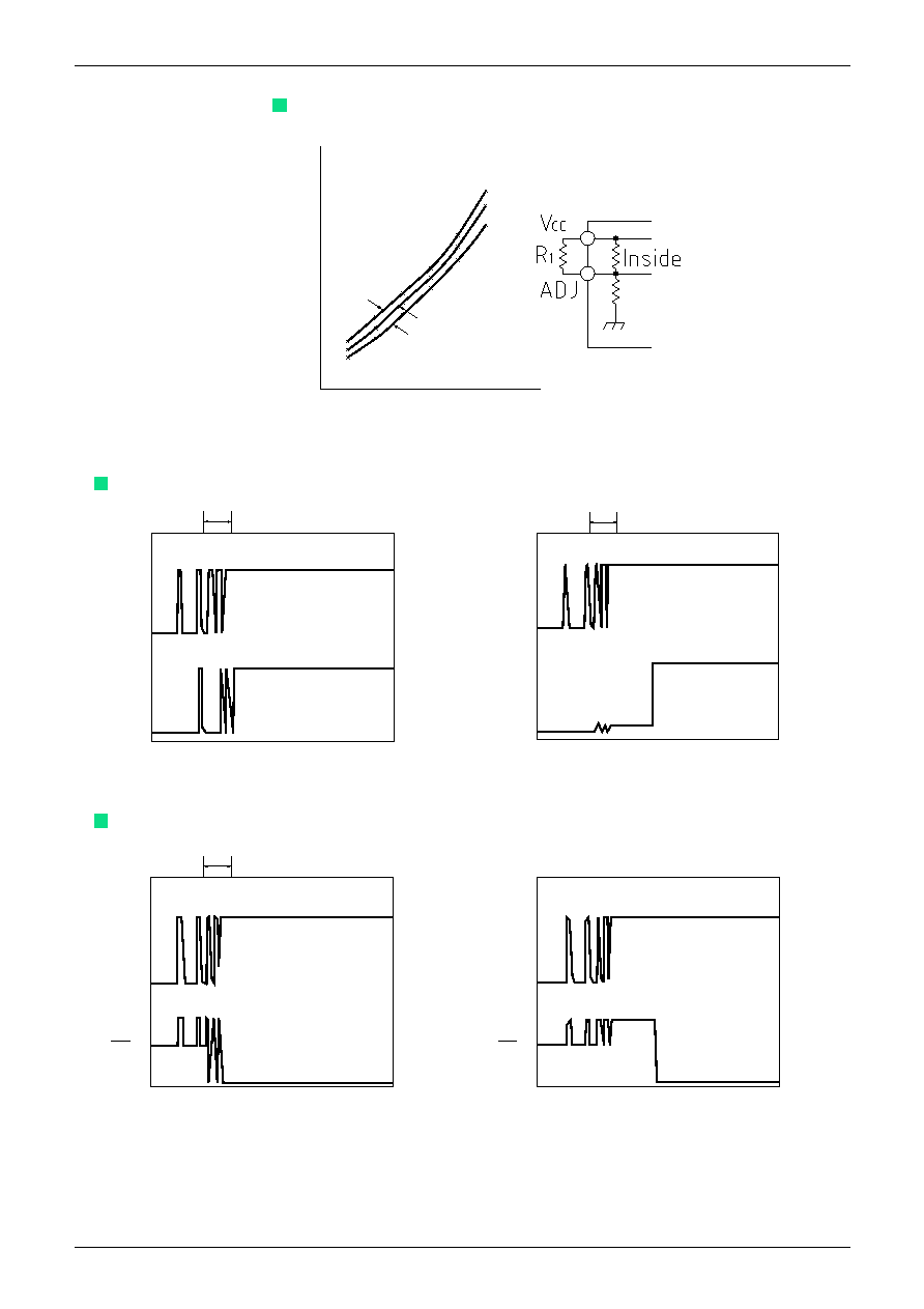
2. Using resistors to divide Vcc potential and connect
to ADJ pin
Detection voltage can be determined close to
external resistance value by setting external R2
and R3 values small.
Refer to Figure 2
(However, current increases when R
2
and R
3
are
made smaller, so set at around R
2
+R
3
=6k
.)
MITSUMI
System Reset (with battery back-up) MM1027, 1081
CS Output
0.5mS
2V/Div
V
CC
CS
*
TC pin OPEN
0.5mS
2V/Div
V
CC
CS
*
TC pin 1000pF
CS
------------------------------------------
Output
0.5mS
2V/Div
V
CC
CS
*
TC pin OPEN
V
CC
CS
*
TC pin 1000pF
CS detection voltage adjustment (ADJ pin)
CS detection voltage
adjustment (ADJ pin)
5
4
3
0
1
2
3
4
max.
typ.
min.
Detection voltage
Resistor R2 (k
)

MITSUMI
System Reset (with battery back-up) MM1027, 1081
Characteristics
(MM1081 series)
Input/output voltage difference 1
(Vcc=5.0V)
4.0
4.5
5.0
50 60 70 80 90 100 110 120 130 140 150
Output voltage (V)
Output current (mA)
CS-CS
---------------------------
detection voltage-Temperature
4.30
4.25
4.20
4.15
4.10
(V)
-25
0
25
50
75
TEMP(
∞
C)
H L
L H
V
CC
-I
CC
V
OUT
-CS
47k
CS open
0.0000
5.000
.5000/div
V
CC
(V)
I
CC
(
µ
A)
300.0
30.00/div
.0000
Power supply switching voltage-Temperature
3.45
3.40
3.35
3.30
3.25
-25
0
25
50
75
TEMP(
∞
C)
(V)
H L
L H
Timing Chart
V
CC
V
BATT
V
OUT
CS
B
D
1,B
D
2
D.CONT:OPEN
B
D
1
D.CONT:GNO
B
D
2
D.CONT:GNO
CS
3.4V
3.6V 4.3V
5V
4.2V 3.5V
3.3V
3.4V3.6V
4.3V
4.2V
2.53V
2.38V
2.35V
2.50V
3.0V
3.5V3.3V
The broken lines for CS and CS
-
-----------------------------------------------------
indicate timing when the ADJ pin is pulled up
to V
CC
by 12k
.