MITSUMI
Sync Detector MM1069
Sync Detector
Monolithic IC MM1069
Outline
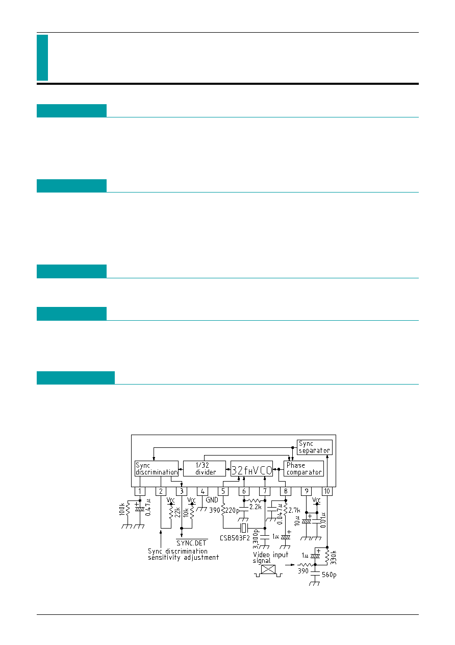
This IC is a sync detection circuit for obtaining the best reception state on VCR and TV channel selection
systems. A system with high detection precision and no adjustment required can be configured due to the
PLL format using a ceramic resonator. It can also be used in OSD circuits for blue-back switching and the
like.
Features
1. Can be used in VCR and TV channel selection systems, and also for blue-back, etc.
2. High precision due to use of PPL format
3. Ceramic resonator means no adjustment required
4. Ceramic resonator can be selected for use in either PAL or NTSC
5. Power supply voltage V
CC
=5V
Package
SIP-10A (MM1069XS)
Applications
1. TV
2. VCR
3. Other video equipment
Block Diagram
MM1069XS

MITSUMI
Sync Detector MM1069
Electrical Characteristics
(Except where noted otherwise, Ta=25�C, V
CC
=5.0V, X=CSB503F2,
R=390 [OHM], C=3300pF, SW1=OFF)
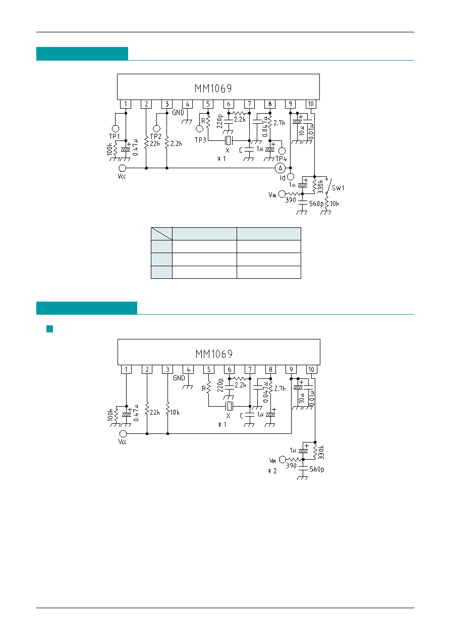
*
1 Signal 1 : Pulse signal with 0.3V amplitude and pulse width 4.7�S
*
2 Measuring horizontal sync signal pull-in range for NTSC
Adjust signal 1 frequency toward 15.734kHz. The measurement value is the smaller of signal 1 frequency
when TP2 level switches from high to low, and the difference from 15.734.
*
3 Measuring horizontal sync signal pull-in range for PAL
Adjust signal 1 frequency toward 15.625kHz. The measurement value is the smaller of signal 1 frequency
when TP2 level switches from high to low, and the difference from 15.625.
*
4 Measuring sync separation level
Gradually lower staircase wave signal sync tip level, and measure sync tip level when TP2 level switches
from low to high.
*
5 Sync discrimination switching voltage measurement
Gradually change the voltage impressed on TP1, and measure TP5 voltage when TP2 output switches.
Signal 1 waveform
4.7uS
Item
Symbol
Measurement
Measurement conditions
Min. Typ. Max. Units
circuit
Operating power supply voltage
V
CC
V
CC
4.7
5.0
5.3
V
Consumption current
Id
Id
7.5
11.0 mA
32fH VCO free-running
f
O
1
TP3
497.1 503.5 509.9 kHz
frequency NTSC
Horizontal sync signal
f
CAP
V
IN
V
IN
: signal 1
*
1
*
2
300
500
Hz
acquisition range NTSC
32fH VCO free-running
f
O
2
TP3
X=CSB500F40, R=200OHM,
frequency PAL
C=4700pF
493.6 500.0 506.4 kHz
Horizontal sync signal
f
CAP
2
V
IN
X=CSB500F40, R=200OHM,
acquisition range PAL
C=4700pF, V
IN
: signal 1
*
1
*
3
300
500
Hz
LPF pin DC level
V
LPF
TP4
SW1 : ON
0.9
1.4
1.9
V
Sync separation level
V
SEPA
V
IN
V
IN
: staircase wave 1V
P-P
*
4
20
50
80
mV
Sync discrimination
V
L
4
TP2
V
IN
: staircase wave 1V
P-P
*
5
0.2
0.4
V
output voltage L
Sync discrimination
V
H
4
TP2
V
IN
: no input signal
*
5
4.8
5.0
V
output voltage H
Sync discrimination
V
THL
4
TP1
TP1 : DC voltage 5V Low
*
5
2.0
2.3
2.6
V
switching voltage L
Sync discrimination
V
THH
4
TP1
TP1 : DC voltage 0V High
*
5
2.7
3.0
3.3
V
switching voltage H

MITSUMI
Sync Detector MM1069
NTSC
PAL
X
CSB503F2
CSB500F40
R
390
220
C
3300pF
4700pF
Note 1 : 1.
*
1
Note 2 :
*
2
1. Input signal sync tip must be less than 1V for
application circuit 1 Pin 10 external circuit.
2. The above 1. does not apply for application circuit
2 Pin 10 external circuit. Pin 10 is clamped at
approximately 2.5V.
Application Circuit 2


