 | ÐлекÑÑоннÑй компоненÑ: MM1075 | СкаÑаÑÑ:  PDF PDF  ZIP ZIP |
Äîêóìåíòàöèÿ è îïèñàíèÿ www.docs.chipfind.ru

MITSUMI
System Reset (with built-in watchdog timer) MM1075
System Reset (with built-in watchdog timer)
Monolithic IC MM1075
Outline
This IC functions in a variety of CPU systems and other logic systems to generate a reset signal and reset the
system accurately during momentary interruption or lowering of power supply voltage.
It also has a built-in watchdog timer for operation diagnosis. This prevents the system from running wild by
generating an intermittent reset pulse during system mis-operation.
Features
1. Built-in watchdog timer
2. Low minimum operating voltage
V
CC
=0.8V typ.
3. Both positive and negative logic reset output can be extracted
4. Accurate detection of drop in power supply voltage
5. Detection voltage has hysteresis
6. Few external parts
1 capacitor
7. Timer monitoring time can be varied by using an external resistor
Package
DIP-8A (MM1075XD)
SOP-8A (MM1075XF)
Applications
Microcomputer system monitoring, etc.
Absolute Maximum Ratings
(Ta=25
°
C)
Item
Symbol
Rating
Units
Storage temperature
T
STG
-40~+125
°
C
Operating temperature
T
OPR
-20~+70
°
C
Power supply voltage
V
CC
max.
-0.3~+10
V
Voltage applied to VS & CK pins
V
VS
&V
CK
-0.3~+10
V
Voltage applied to RESET, RESET
--------------------------------------------------------------
pin
V
OH
-0.3~+10
V
Allowable loss
Pd
400
mW
MITSUMI
System Reset (with built-in watchdog timer) MM1075
Electrical Characteristics (DC)
(Except where noted otherwise, Ta=25°C, V
CC
=5V)
Item
Symbol
Measurement
Measurement conditions
Min. Typ. Max.
Units
circuit
Consumption current
I
CC
1
During watchdog timer operation
0.7
1.0
mA
Detection voltage
V
SL
1
4.05
4.20
4.35
V
V
SH
1
4.15
4.30
4.45
Detection voltage
V
S
/ T
1
±0.01
%/
°
C
temperature coefficient
Hysteresis voltage
V
HYS
1
50
100
150
mV
CK input threshold
V
TH
1
0.8
1.2
2
V
CK input current
I
IH
1
V
CK
=5V
0
1
µA
I
IL
1
V
CK
=0V
-20
-10
-3
Output voltage (High)
V
OH
1
1
I
=-5µA, V
S
=OPEN
4.5
4.8
V
V
OH
2
1
I
=-5µA, V
S
=0V
4.5
4.8
V
OL
1
1
I
=3mA, V
S
=0V
0.2
0.4
Output voltage (Low)
V
OL
2
1
I
=10mA, V
S
=0V
0.3
0.5
V
V
OL
3
1
I
RESET
=0.5mA, V
S
=OPEN
0.2
0.4
V
OL
4
1
I
RESET
=1mA, V
S
=OPEN
0.3
0.5
Output sink current
I
OL
1
1
V
=1.0V, V
S
=0V
10
16
mA
I
OL
2
1
V
RESET
=1.0V, V
S
=OPEN
1
2
I
CT
1
1
V
TC
=1.0V, R
CT
=OPEN during
C
T
charge current
*
1
watchdog timer operation
-0.8
-1.2
-2.4
µA
I
CT
2
1
V
TV
=1.0V during power ON
reset operation
-0.8
-1.2
-2.4
µA
Minimum operating power supply
voltage to ensure RESET
----------------------------------------------------------------------------
V
CCL
1
1
0.8
1.0
V
Minimum operating power supply
V
CCL
2
1
voltage to ensure RESET
0.8
1.0
V
RESET
----------------------------------------------------------------
RESET
----------------------------------------------------------------
RESET
----------------------------------------------------------------
RESET
----------------------------------------------------------------
RESET
----------------------------------------------------------------
V
RESET
=V
CC
-0.1V
R
L
2 (between Pin 2 and GND)
V
=0.4V
I
=0.2mA
RESET
----------------------------------------------------------------
RESET
----------------------------------------------------------------
V
S
=OPEN, V
CC
V
S
=OPEN, V
CC
V
SH
-V
SL
, V
CC
MITSUMI
System Reset (with built-in watchdog timer) MM1075
Electrical Characteristics (AC)
(Except where noted otherwise, Ta=25°C, V
CC
=5V)
Item
Symbol
Measurement
Measurement conditions
Min. Typ. Max.
Units
circuit
V
CC
input pulse width
T
P
1
2
8
µS
CK input pulse width
T
CKW
2
3
µS
CK input cycle
T
CK
2
20
µS
Watchdog timer
T
WD
2
C
T
=0.1µF
monitoring time
*
2
R
CT
=OPEN
50
100
150
mS
Reset time for
watchdog timer
*
3
T
WR
2
C
T
=0.1µF
1
2
3
mS
Reset hold time for
power supply rise
*
4
T
PR
2
50
100
150
mS
Output delay time
T
PD
1
2
RESET pin
from V
CC
R
L
1=2.2k
, C
L
1=100pF
2
10
µS
*
5
T
PD
2
2
RESET pin
R1, 2=10k
, C
L
2=20pF
3
10
t
R
1
2
RESET pin
Output rise time
R
L
1=2.2k
, C
L
1=100pF
1.0
1.5
µS
*
6
t
R
2
2
RESET pin
R
L
2=10k
, C
L
2=20pF
1.0
1.5
µS
t
F
1
2
RESET pin
Output fall time
R
L
1=2.2k
, C
L
1=100pF
0.1
0.5
µS
*
6
t
F
2
2
RESET pin
R
L
2=10k
, C
L
2=20pF
0.5
1.0
µS
V
CC
5V
4V
Notes:
*
1 I
CT
1 changes according to R
CT
pin (Pin 6) pull up resistance.
*
2 Monitoring time is the time from the last pulse (negative edge) of the timer clear clock pulse until reset
pulse output. In other words, reset output is output if a clock pulse is not input during this time. Also,
monitoring time can be varied by pulling up the R
CT
pin to V
CC
with a resistor (R
CT
). Monitoring time
adjustments are shown in Graph 1.
*
3 Reset time means reset pulse width. However, this does not apply to power ON reset.
*
4 Reset hold time is the time from when V
CC
exceeds detection voltage (V
SH
) during power ON reset until
reset release (RESET
--------------------------------------------------------------
output high, RESET output low).
*
5 Output delay time is the time from when power supply voltage drops below detection voltage (V
SI
) until
reset (RESET
--------------------------------------------------------------
output low, RESET output high).
*
6 Voltage range when measuring output rise and fall is 10~90%.
*
7 Watchdog timer monitoring time (T
WD
), watchdog timer reset time (T
WR
) and reset hold time (T
PR
) during
power supply rise can be changed by varying C
T
capacitance. The times are expressed by the following
formulae. The recommended range for C
T
is 0.001~10µF.
T
PR
(mS) ~
- 1000 C
T
(µF)
T
WD
(mS) ~
- 1000 C
T
(µF)
T
WR
(mS) ~
- 20 C
T
(µF)
Example : When C
T
=0.1µF (R
CT
pin OPEN)
T
PR
~
- 100mS
T
WD
~
- 100mS
T
WR
~
- 2mS
CK
or
C
T
=0.1µF, V
CC
MITSUMI
System Reset (with built-in watchdog timer) MM1075
(mS)
100
80
60
40
20
0
50k 100k
1M
10M
100M
(
)
T
WD
R
CT
Graph 1 R
CT
& Monitoring Time
Note : The above graph shows data for when C
T
=0.1µF.
T
WD
is proportionate to C
T
. Refer to the calculation formula for T
WD
above.
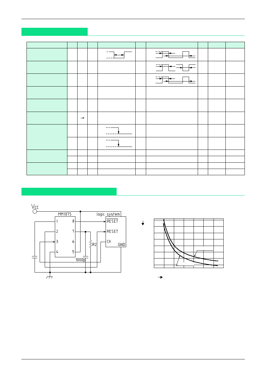
Block Diagram
Note 1 : CP=0.1µF approx.
Note 2 : C~
-1000pF
Note 3 : The watchdog timer can be stopped by connecting the RCT pin to
GND. (Then it functions as a voltage detection circuit.)
Note 4 : T
PR
and T
WD
can be varied by pulling up the R
CT
pin to V
CC
with a
resistor. The recommended range for RCT is 100k
~R
CT
pin OPEN.
MITSUMI
System Reset (with built-in watchdog timer) MM1075
Timing Chart
V
CC
CK
C
T
RESET
RESET
V
SH
V
SL
T
PR
T
WD
T
CK
T
WR
Pin Assignment
1
4
3
2
8
5
6
7
1
TC
2
RESET
3
CK
4
GND
5
V
CC
6
RCT
7
V
S
8
RESET
-----------------------------------------------------------------------------
Pin Description
Pin No. Pin Name
Function
1
TC
T
WD
, T
WR
, T
PR
variable pins.(T
WD
, T
WR
and T
PR
times are determined by the external capacitor.)
2
RESET
Reset output pin (High output)
3
CK
Clock input pin (inputs clock from logic system)
4
GND
5
V
CC
4.2V detection voltage
6
RCT
Watchdog timer stop pin Operation modes : Operation OPEN, Stop connect to GND
7
V
S
Detection voltage variable pin Adjustment modes : Lower pull up resistance, Raise pull down
8
RESET
---------------------------------------------------------------
Reset output pin (Low output)
MITSUMI
System Reset (with built-in watchdog timer) MM1075
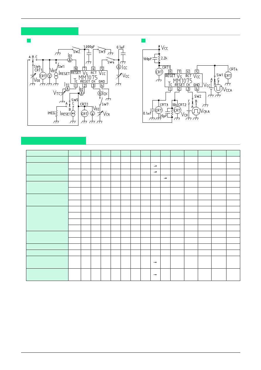
Measuring Circuits
Measuring Circuit 1
Measuring Circuit 2
Measuring Circuit 2-1
SW & Power Supply Table
Item
Symbol SW1 SW2 SW3 SW4 SW5 SW6 SW7 V
CC
V
CK
V
CT
I
I
RESET
VM, IM Notes
Consumption current
I
CC
OFF OFF OFF ON
B
B
ON
5V
5V
0V
-
-
I
CC
Detection voltage
V
SL
OFF OFF ON
ON
B
B
ON 5V 4V 3V
3V
-
-
V
O
1, CRT1
V
SH
OFF OFF ON
ON
B
B
ON 4V 5V 3V
3V
-
-
V
O
1, CRT1
CK input threshold
V
TH
OFF OFF OFF ON
B
B
ON
5V 0V 3V
1V
-
-
I
CK
CK input current
I
IH
OFF OFF OFF ON
B
B
ON
5V
5V
0V
-
-
I
CK
I
IL
OFF OFF OFF ON
B
B
ON
5V
0V
0V
-
-
I
CK
Output voltage
V
OH
1
ON OFF ON
ON
B
B
ON
5V
5V
3V
-5µA
-
V
O
1
(High)
V
OH
2
OFF ON
ON
ON
C
B
ON
5V
5V
3V
-
-5µA
V
O
2
V
OL
1
ON
ON
ON
ON
B
B
ON
5V
5V
3V
3mA
-
V
O
1
Output voltage
V
OL
2
ON
ON
ON
ON
B
B
ON
5V
5V
3V
10mA
-
V
O
1
(Low)
V
OL
3
OFF OFF ON
ON
C
B
ON
5V
5V
3V
-
0.5mA
V
O
2
V
OL
4
OFF OFF ON
ON
C
B
ON
5V
5V
3V
-
1mA
V
O
2
Output sink current
I
OL
1
OFF ON
ON
ON
B
C
ON
5V
5V
3V
-
-
I
O
1
V
OO
=1V
I
OL
2
OFF OFF ON
ON
B
A
ON
5V
5V
3V
-
-
I
O
2
V
OO
=1V
C
T
charge current 1
I
TC
1
OFF OFF OFF ON
B
B
OFF
5V
-
1V
-
-
I
TC
C
T
charge current 2
I
TC
2
OFF OFF ON
ON
B
B
OFF
5V
-
1V
-
-
I
TC
Minimum operating power supply
voltage to ensure RESET
----------------------------------------------------------
V
CCL
1
ON OFF ON
ON
B
B
ON 0V 2V 0V
0V
-
V
O
1, V
CC
Minimum operating power supply
voltage to ensure RESET
V
CCL
2 OFF ON
ON
ON
A
B
ON 0V 2V 0V
0V
-
-
V
O
2, V
CC
RESET
-
------------------------------------------------------------
MITSUMI
System Reset (with built-in watchdog timer) MM1075
Measuring Circuit 2-2
SW & Power Supply Table
Item
Symbol SW1 SW2
V
CCA
V
CC
V
CKA
V
CK
CRT
Notes
V
CC
input pulse width
T
PI
C
B
-
-
CRT1, 2, 3
T1=8µS
CK input pulse width T
CKW
A
B
-
5V
-
CRT1, 2, 3
T2=3µS
CK input cycle
T
CK
A
B
-
5V
-
CRT1, 2, 3
T3=20µS
Watchdog timer
monitoring time
T
WD
A
A
-
5V
-
5V
CRT1, 2, 3
Reset time for
watchdog timer
T
WR
A
A
-
5V
-
5V
CRT1, 2, 3
Reset hold time for
power supply rise
T
PR
B A
A
-
5V
-
5V
CRT1, 2, 3
T
PD
1
C
A
-
-
0V
CRT1, 3
Output delay time
from V
CC
T
PD
2
C
A
-
-
0V
CRT2, 3
Output rise time
T
R
1
A
A
-
5V
-
5V
CRT1
T
R
2
A
A
-
5V
-
5V
CRT2
Output fall time
T
P
1
A
A
-
5V
-
5V
CRT1
T
P
2
A
A
-
5V
-
5V
CRT2
5V
4V
T1
1.4V
0V
T2
T3
1.4V
0V
T2
T2
or
5V
0V
5V
0V
1.4V
0V
T2
T3
Detection Voltage Adjustment 1
(lowering detection voltage)
Vs pin external resistance
(R2) (k
)
5.0
4.5
100 200 300 400 500 600
Detection voltage
(Vs) (V)
V
SH
value
V
SL
value
Detection voltage can be changed by
connecting resistor R2 externally to
MM1075 V
S
pin. Determine R2 according to
graph 1 when changing V
S
.
Graph 1. Detection voltage change using MM1075
external resistor
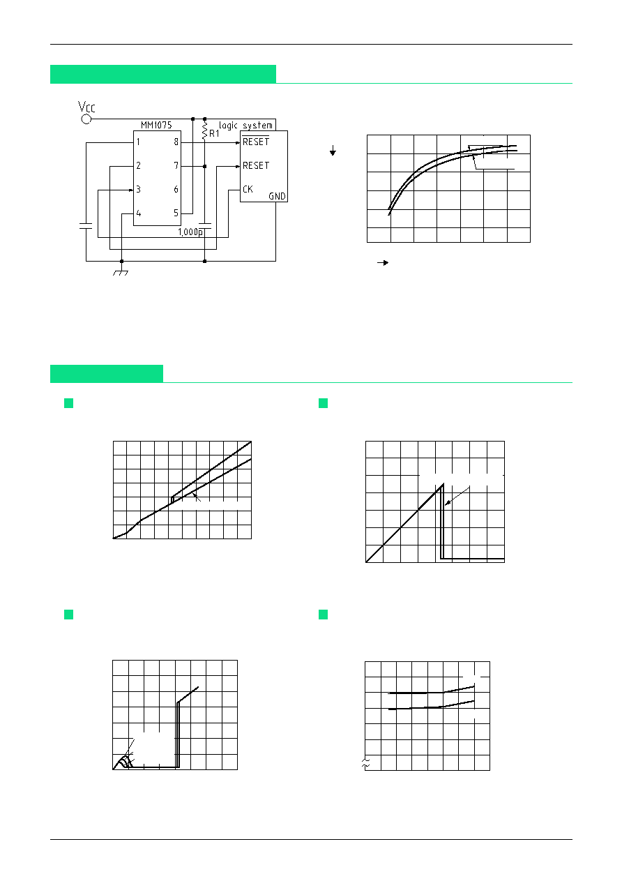
MITSUMI
System Reset (with built-in watchdog timer) MM1075
(raising detection voltage)
Detection Voltage Adjustment 2
Detection voltage can be changed by
connecting resistor R1 externally to
MM1075 V
S
pin. Determine R1 according
to graph 2 when changing V
S
.
Vs pin external resistance
(R1) (k
)
V
SL
value
4.0
3.5
3.0
100 200 300 400 500 600
Detection voltage
(V
S
) (V)
V
SH
value
Graph 2. Detection voltage change using MM1075
external resistor
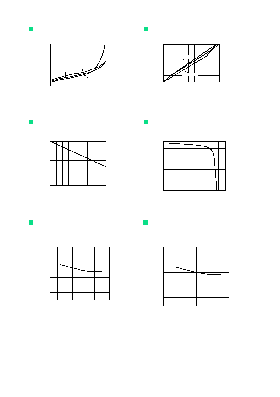
Characteristics
V
SH
V
SL
4.50
4.40
4.30
4.20
4.10
4.00
3.90
-40-20 0 20 40 60 80 100
Detection voltage (V)
Ambient temperature Ta (
°
C)
Ta=-25
°
C
Ta=25
°
C
Ta=75
°
C
7.0
6.0
5.0
4.0
3.0
2.0
1.0
1.0 2.0 3.0 4.0 5.0 6.0 7.0 8.0
Output voltage
V
RESET
(V)
Power supply voltage
V
CC
(V)
PULL UP resistance 2.2k
Output voltage-Power supply
voltage (RESET pin)
Detection voltage (V
SL
, V
SH
) temperature
(RESET, RESET
-----------------------------------------------------------------
pins)
7.0
6.0
5.0
4.0
3.0
2.0
1.0
1.0 2.0 3.0 4.0 5.0 6.0 7.0 8.0
Ta=20
°
C, 25
°
C, 75
°
C
Power supply current
I
CC
(mA)
Power supply voltage
V
CC
(V)
PULL UP resistance 10k
1.4
1.2
1.0
0.8
0.6
0.4
0.2
1.0 2.0 3.0 4.0 5.0 6.0 7.0 8.0 9.0 10.0
Power supply current
I
CC
(mA)
Power supply voltage
V
CC
(V)
Clock pulse input time
Power supply current-Power supply
voltage
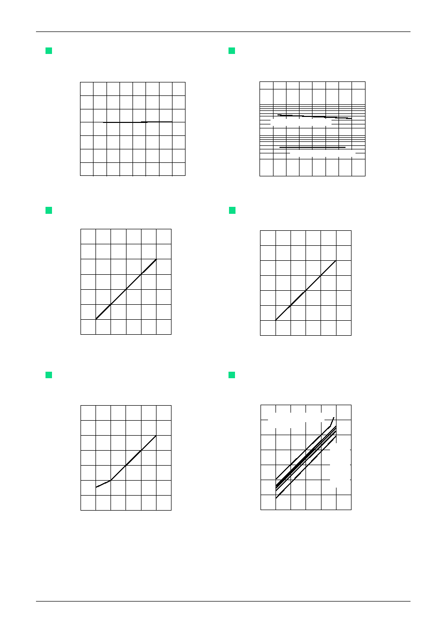
Output voltage-Power supply voltage
(RESET pin)
MITSUMI
System Reset (with built-in watchdog timer) MM1075
500
400
300
200
100
0.2 0.4 0.6 0.8 1.0 1.4 1.6 1.8
Ta=75
°
C
Ta=-25
°
C
Ta=25
°
C
Output saturation voltage
V
OL
(mV)
Output sink current
I
OL
(mA)
Output saturation voltage-Output sink current
(RESET
------------------------------------------------------------------------
pin)
500
400
300
200
100
2
4
6
8 10 12 14 16 18
Ta=25
°
C
Ta=-25
°
C
Ta=75
°
C
Output saturation voltage
V
OL
(mV)
Output sink current I
OL
(mA)
Output saturation voltage-Output sink current
(RESET
-----------------------------------------------------------------
pin)
5.0
4.8
4.6
4.4
4.2
4.0
3.8
-2 -4 -6 -8-10-12-14 -16-18
High level output voltage
V
OM
(V)
High level output current
I
OM
(
µ
A)
High level output voltage-High level output
current (RESET pin)
High level output voltage
V
OM
(V)
5.0
4.8
4.6
4.4
4.2
4.0
3.8
-2 -4 -6 -8-10-12-14 -16 -18
High level output current
I
OM
(
µ
A)
High level output voltage-High level output
current (RESET
-----------------------------------------------------------
pin)
160
140
120
100
80
60
40
-40-20 0
20 40 60 80 100
V
CC
=5V (Cr=0.1
µ
F)
Reset hold time temperature during
power supply rise T
PR (
mS)
Ambient temperature Ta (
°
C)
Reset hold time temperature during power
supply rise
160
140
120
100
80
60
40
-40 -20 0
20
40 60 80 100
V
CC
=5V (Cr=0.1
µ
F)
Watchdog timer monitoring time
temperature T
WD
(mS)
Ambient temperature Ta (
°
C )
Watchdog timer monitoring time
temperature
MITSUMI
System Reset (with built-in watchdog timer) MM1075
10
5
10
4
10
3
10
2
10
1
10
-3
10
-2
10
-1
10
0
10
0
10
1
Hold time T
PR
(mS)
C
T
capacitance (
µ
F)
C
T
value for reset hold time during power
supply rise
10
3
10
2
10
1
10
0
10
-1
10
-2
10
-3
10
-2
10
-1
10
0
10
1
Reset time T
WR
(mS)
C
T
capacitance (
µ
F)
C
T
value for reset time (for watchdog timer)
10
5
10
4
10
3
10
2
10
1
10
0
10
-3
10
-2
10
-1
10
0
10
1
Timer monitoring time T
WD
(mS)
C
T
capacitance (
µ
F)
C
T
value for watchdog timer monitoring
time
R=
OPEN
2.2M
1k
470k
200k
10
3
10
2
10
1
10
0
10
-1
10
4
10
-3
10
-2
10
-1
10
0
10
1
Timer monitoring time T
WD
(mS)
C
T
capacitance (
µ
F)
Connect R between
Rct and V
CC
Type of timer time adjustment
C
T
value for watchdog timer monitoring time
3.5
3.0
2.5
2.0
1.5
1.0
0.5
-40 -20
0
20 40 60
80 100
V
CC
=5V (Cr=0.1
µ
F)
Reset time T
WR
(mS)
Ambient temperature Ta (
°
C)
Reset time temperature
(for watchdog timer)
6PIN 100k
PULL UP
6PIN 5M
PULL UP
V
CC
=5V (Cr=0.1
µ
F)
100
10
-40 -20 0
20 40 60
80 100
Ambient temperature Ta (
°
C)
Watchdog timer monitoring time
temperature