MITSUMI
4fsc Clock Generator MM1093
4fsc Clock Generator
Monolithic IC MM1093
Outline
This IC generates a clock used for driving the CCD that configures a comb filter for Y/C separation, or for
sampling A/D and D/A converters that configure a digital comb filter.
It has a built-in subcarrier oscillator (3.58MHz or 4.43MHz) synchronized to the input chroma signal, and a
clock oscillator that is 4 times the latter. MM1093ND and NF are available for NTSC format, and MM1093PD
and PF for PAL format.
Features
1. Built-in fsc synchronized to input chroma signal and 4fsc oscillators
2. Reduced number of external parts due to 1 pin VCXO
3. +5V single power supply
Package
SOP-16A (MM1093NF, MM1093PF)
DIP-16B (MM1093ND, MM1093PD)
Applications
1. TV
2. VCR
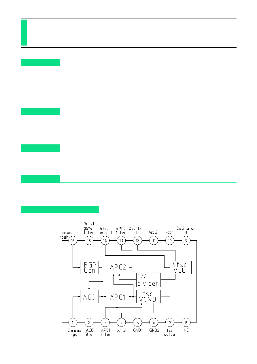
Equivalent Circuit Diagram

MITSUMI
4fsc Clock Generator MM1093
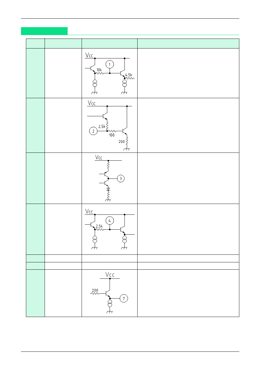
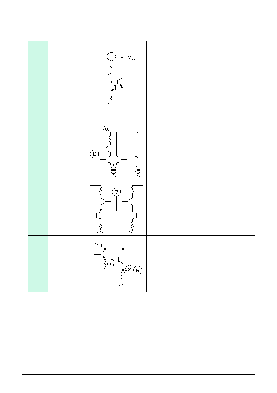
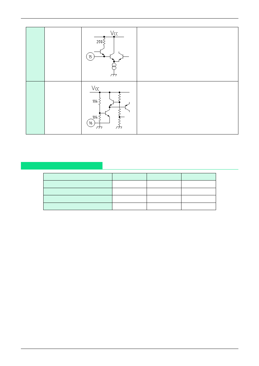
Pin Description
Pin no.
Pin name
Equivalent Circuit Diagram
Pin Description
1
Chroma input
2
ACC filter
3
APC1 filter
4
X'tal
Chroma signal input pin
ACC filter pin
fsc APC circuit filter pin
VCXO circuit X'tal pin
5
GND1
fsc GND pin
6
GND2
4fsc GND pin
7
fsc output
Outputs subcarrier synchronized to input
chroma signal
NTSC : 3.579545MHz
PAL : 4.433619MHz

MITSUMI
4fsc Clock Generator MM1093
8
NC
9
Oscillator R
10
V
CC
1
11
V
CC
2
NC pin
fsc power supply pin
4fsc power supply in
13
APC2 filter
4fsc APC circuit filter pin
Connects to resistor that determines 4fsc VCO
free run frequency
12
Oscillator C
Connects to capacitor that determines 4fsc
VCO free run frequency
14
4fsc output
Outputs a 4 signal sychronized to input
chroma signal.

MITSUMI
4fsc Clock Generator MM1093
Item
Symbol
Measurement
Measurement conditions
Min. Typ. Max. Units
circuit
Operating power supply voltage
V
CC
V
CC
4.7
5.0
5.3
V
Consumption current
I
CC
-
24
32
mA
Sync separation circuit
SG2 : 1V
P-P
staircase wave
*
1
Sync separation level
V
S
TP3
SG1 : separate chroma signal
40
80
120
mV
SW1 : B
*
5
PLL circuit
ACC input amplitude range
V
IN
TP1
SG1 : separate chroma signal
*
2
*
5
15
560 mV
P-P
APC1 frequency
f
C
SG1 : sine wave 143mV
P-P
400
Hz
acquisition range
SG2 : 1V
P-P
staircase wave
*
3
VCO1 free run frequency deviation
f0
*
4
-250
0
250
Hz
fSC output level
V
O
1
TP2
SG1 : separate chroma signal
SG2 : 1V
P-P
staircase wave
*
5
0.8
1.0
1.2
V
P-P
fSC output duty
D
O
1
SG1 : separate chroma signal
SG2 : 1V
P-P
staircase wave
*
5
45
50
55
%
4fSC circuit
SG1 : separate chroma signal
4fSC output level
V
O
2
SG2 : 1V
P-P
staircase wave
0.8
1.0
1.2
V
P-P
SW1 : B
*
5
SG1 : separate chroma signal
4fSC output DT
D
O
2
TP3
SG2 : 1V
P-P
staircase wave
45
50
55
%
SW1 : B
*
5
SG1 : separate chroma signal
fSC leakage
Lfsc
SG2 : 1V
P-P
staircase wave
50
dB
SW1 : B
*
5
Electrical Characteristics
(Except where noted otherwise, Ta=25∞C, V
CC
=5.0V, SG1, SG2 : no signal, SW1 : A)
Notes:
*
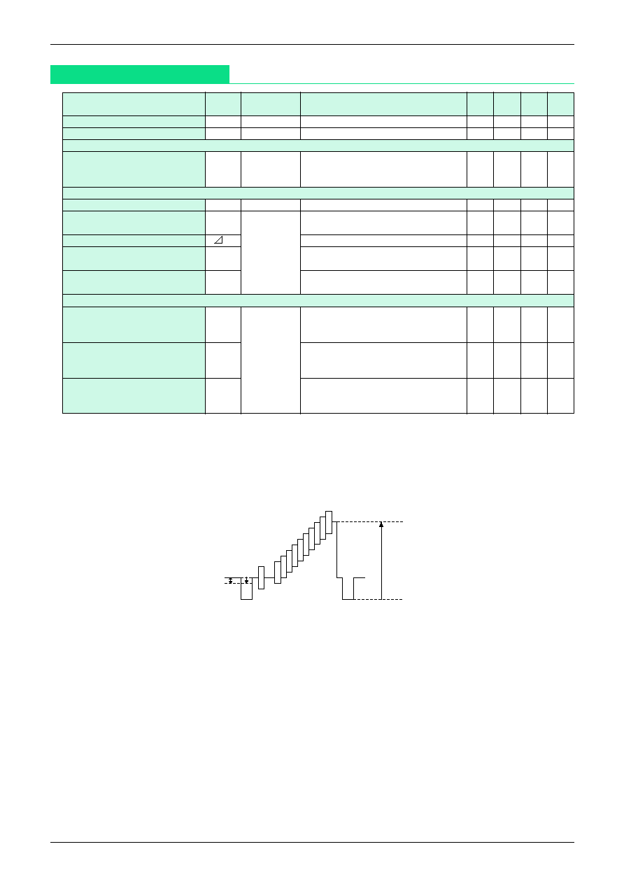
1 Sync separation level
Measure the level where SG1 input signal and TP3 output signal synchronize when 1V
P-P
staircase wave
sync signal level is raised from 0V.
1V
P-P
V
S
Hsync
*
2 ACC input amplitude range
Defined as separate chroma signal burst signal amplitude that can be input to chroma input.
*
3 APC1 frequency pull-in range
Defined as the smaller of the differences when input signal frequency is changed from high to f
O
and from
low to fo when TP2 output is not synchronized to SG1 input signal and when it is synchronized.
*
4 VCO1 free run frequency deviation
Defined as the difference between TP2 output signal frequency and f
O
.
*
5 The standard for the separate chroma signal is burst signal 143mV
P-P
.
SG2 : 1V
P-P
staircase wave
