 | –≠–ª–µ–∫—Ç—Ä–æ–Ω–Ω—ã–π –∫–æ–º–ø–æ–Ω–µ–Ω—Ç: MM1096A | –°–∫–∞—á–∞—Ç—å:  PDF PDF  ZIP ZIP |
MITSUMI
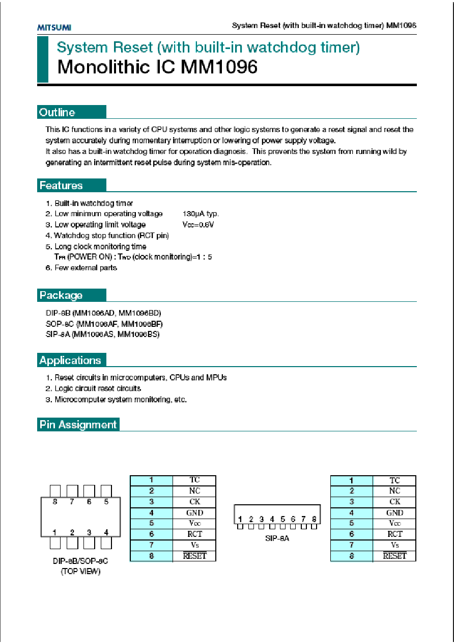
System Reset (with built-in watchdog timer) MM1096
Electrical Characteristics (DC)
(Except where noted otherwise, MM1096A : V
CC
=3.6V, Ta=25∞C, MM1096B : V
CC
=5.0V)
Item
Symbol
Measurement conditions
Min. Typ. Max. Units
Consumption current
MM1096A
I
CC
During watchdog timer operation
100
150
µA
MM1096B
130
195
MM1096A
V
SL
3.10 3.20 3.30
Detection voltage
MM1096B
4.05 4.20 4.35
V
MM1096A
V
SH
3.15 3.25 3.35
MM1096B
4.15 4.30 4.45
Detection voltage temperature coefficient
V
S
/ T
±0.01
%/
∞
C
Hysteresis voltage
MM1096A
V
HYS
25
50
100
mV
MM1096B
50
100
150
CK input threshold
V
TH
0.8
1.2
2
V
CK input current
I
IH
A : V
CK
=3.6V, B : V
CK
=5.0V
0
1
µA
I
IL
V
CK
=0V
-12
-6
-2
Output voltage
MM1096A
V
OH
I
=1µA
3.0
3.4
V
(High)
MM1096B
V
S
=OPEN
4.0
4.5
Output voltage (Low)
V
OL
1
I
=0.5mA, V
S
=0V
0.2
0.4
V
V
OL
2
I
=1.0mA, V
S
=0V
0.3
0.5
R output sync current
I
OL
V
=1.0V, V
S
=0V
1
2
mA
C
T
charge current
I
CT
1
V
TC
=1.0V during watchdog timer operation -0.28 -0.48 -0.96
µA
I
CT
2
V
TC
=1.0V during power ON reset operation -1.60 -2.40 -4.80
µA
Minimum operating power
supply voltage to ensure RESET
---------------------------------------------------
V
CCL
0.8
1.0
V
RESET
----------------------------------------------------
RESET
----------------------------------------------------
RESET
----------------------------------------------------
RESET
----------------------------------------------------
V
S
=OPEN, V
CC
V
S
=OPEN, V
CC
V
=0.4V
I
=0.1mA
RESET
----------------------------------------------------
RESET
----------------------------------------------------
V
SH
-V
SL
, V
CC
MITSUMI
System Reset (with built-in watchdog timer) MM1096
Electrical Characteristics (DC)
(Except where noted otherwise, MM1096A : V
CC
=3.6V, Ta=25∞C, MM1096B : V
CC
=5.0V)
(Except where noted otherwise, resistance unit is
)
Item
Symbol Measurement
conditions
Min.
Typ.
Max.
Units
MM1096A
8
V
CC
input
T
PI
µs
pulse width
MM1096B
8
CK input pulse width
T
CKW
3
µs
CK input cycle
T
CK
20
µs
Watchdog timer
monitoring time
*
1
T
WD
C
T
=0.02µF
25
50
75
ms
Reset time for
watchdog timer
*
2
T
WR
C
T
=0.02µF
1
2
3
ms
Reset hold time for
power supply rise
*
3
T
PR
5
10
15
ms
Output delay time from V
CC
*
4
T
PD
RESET
--------------------------------------------------------------------------
pin, R
L
=10k, C
L
=20pF
2
10
µs
Output rise time
*
5
t
R
RESET
--------------------------------------------------------------------------
pin, R
L
=10k, C
L
=20pF
2.0
4.0
µs
Output fall time
*
5
t
F
RESET
--------------------------------------------------------------------------
pin, R
L
=10k, C
L
=20pF
0.2
1.0
µs
V
CC
3.6V
2.8V
V
CC
5.0V
4.0V
C
T
=0.02µF, V
CC
Notes:
*
1 Monitoring time is the time from the last pulse (negative edge) of the timer clear clock pulse until reset
pulse output. In other words, reset output is output if a clock pulse is not input during this time.
*
2 Reset time means reset pulse width. However, this does not apply to power ON reset.
*
3 Reset hold time is the time from when V
CC
exceeds detection voltage (V
SH
) during power ON reset until
reset release (RESET
-----------------------------------------------
output high).
*
4 Output delay time is the time from when power supply voltage drops below detection voltage (V
SL
) until
reset (RESET
-----------------------------------------------
output low).
*
5 Voltage range when measuring output rise and fall is 10~90%.
*
6 Watchdog timer monitoring time (T
WD
), watchdog timer reset time (T
WR
) and reset hold time (T
PR
) during
power supply rise can be changed by varying C
T
capacitance. The times are expressed by the following
formulae.
T
PR
(ms)
.
=. 500 C
T
(µF)
T
WD
(ms)
.
=. 2500 C
T
(µF)
T
WR
(ms)
.
=. 100 C
T
(µF)
Example : When C
T
=0.02µF
T
PR
.
=. 10ms
T
WD
.
=. 50ms
T
WR
.
=. 2ms
CK
or
MITSUMI
System Reset (with built-in watchdog timer) MM1096
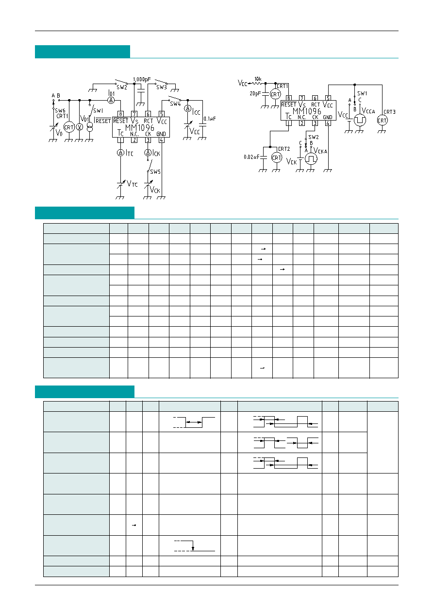
Measuring Circuit 1
SW & Power Supply Table
Measuring Circuit 2
SW & Power Supply Table
Item
Symbol SW1
SW2
SW3
SW4
SW5
SW6
V
CC
V
CK
V
CT
I
VM, IM
Notes
Consumption current
I
CC
OFF
OFF
OFF
ON
ON
A
3.6V
3.6V
0V
I
CC
Detection voltage
V
SL
OFF
OFF
ON
ON
ON
A
3.6V 3V
0V
2V
V
O
1, CRT1
V
SH
OFF
OFF
ON
ON
ON
A
3V 3.6V
0V
2V
V
O
1, CRT1
CK input threshold
V
TH
OFF
OFF
OFF
ON
ON
A
3.6V
0V 3V
1V
I
CK
, V
CK
CK input current
I
IH
OFF
OFF
OFF
ON
ON
A
3.6V
3.6V
0V
I
CK
I
IL
OFF
OFF
OFF
ON
ON
A
3.6V
0V
0V
I
CK
Output voltage (High)
V
OH
ON
OFF
ON
ON
ON
A
3.6V
3.6V
2V
-1µA
V
O
1
Output voltage (Low)
V
OL
1
ON
ON
ON
ON
ON
A
3.6V
3.6V
2V
0.5mA
V
O
1
V
OL
2
ON
ON
ON
ON
ON
A
3.6V
3.6V
2V
1.0mA
V
O
1
Output sink current
I
OL
1
OFF
ON
ON
ON
ON
B
3.6V
3.6V
2V
I
O
1
V
O
=1V
C
T
charge current 1
I
TC
1
OFF
OFF
OFF
ON
OFF
A
3.6V
1V
I
TC
C
T
charge current 2
I
TC
2
OFF
OFF
OFF
ON
OFF
A
3.6V
IV
I
TC
Minimum operating power
supply voltage to ensure RESET
------------------------------------------------------
V
CCL
ON
OFF
ON
ON
ON
A
0V 2V
0V
0V
V
O1
, V
CC
RESET
-----------------------------------------------
Item
Symbol SW1 SW2
V
CCA
V
CC
V
CKA
V
CK
CRT
Notes
V
CC
input pulse width
T
P
1
C
B
-
-
CRT1
T1=8µs
CRT2
CK input pulse width T
CKW
A
B
-
3.6V
-
CRT1
T2=3µs
CRT2
CK input cycle
T
CK
A
B
-
3.6V
-
CRT1
T3=20µs
CRT2
Watchdog timer
T
WD
A
A
-
3.6V
-
3.6V
CRT1
monitoring time
CRT2
Reset time
T
WR
A
A
-
3.6V
-
3.6V
CRT1
for watchdog timer
CRT2
Reset hold time for
T
PR
B A
A
-
3.6V
-
3.6V
CRT1
power supply rise
CRT2
Output delay time
from V
CC
T
PD
C
A
-
-
0V
CRT1
Output rise time
T
R
A
A
-
3.6V
-
3.6V
CRT1
Output fall time
T
F
A
A
-
3.6V
-
3.6V
CRT1
3.6V
2.8V
T1
1.4V
0V
T2
T3
1.4V
0V
T2
T2
or
1.4V
0V
3.6V
0V
T2
T3
Measuring Circuits
Measuring Circuit 1 (DC)
Measuring Circuit 2 (AC)
MITSUMI
System Reset (with built-in watchdog timer) MM1096
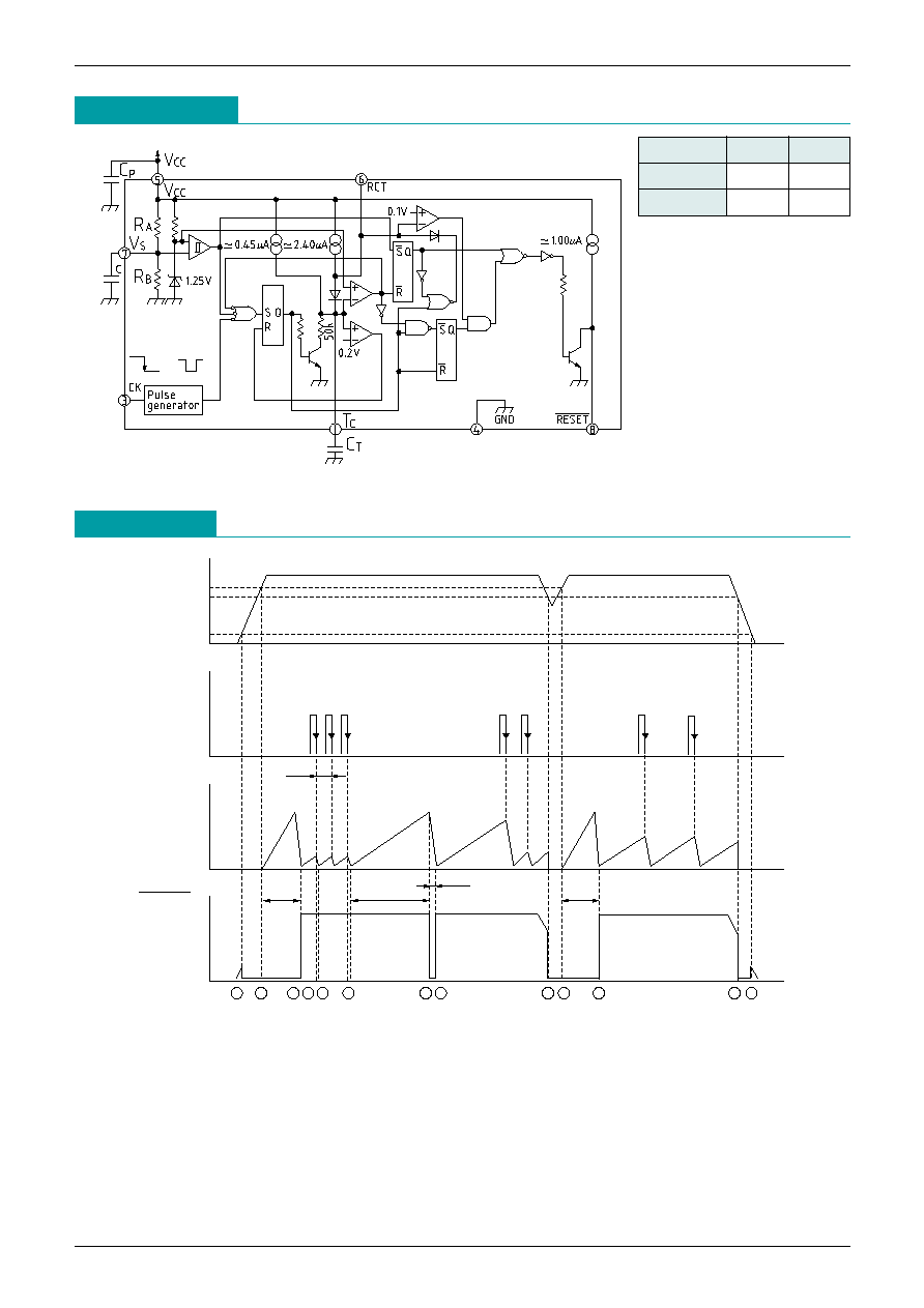
Block Diagram
Timing Chart
V
CC
CK
TC
RESET
V
SL
0.8V
V
SH
T
CK
T
PR
T
WD
T
WR
T
PR
2
1
3 4 5
5
6 7
8
9
10
11
12
Note 1: C
P
=0.1µF approx.
Note 2: C >
= 1000pF
Note 3: The watchdog timer
can be stopped by
connecting the RCT
pin to GND. Then it
functions as a voltage
detection circuit.)
R
A
R
B
MM1096A
~
- 305k ~
- 195k
MM1096B
~
- 350k ~
- 150k
MITSUMI
System Reset (with built-in watchdog timer) MM1096
1. RESET
-------------------------------------------------
goes low when V
CC
rises to approximately 0.8V.
Approximately 1µA (V
CC
=0.8V) of pull up current is output from RESET
-------------------------------------------------
2. Capacitor C
T
charging starts when V
CC
rises to V
SH
(MM1096A
.
=. 3.25V, MM1096B
.
=. 4.3V). Output is in
reset state at this time.
3. Output reset is released (RESET
-----------------------------------------------
goes high) after a certain time (T
PR
), from when C
T
starts charging until
discharge (the time from when C
T
voltage reaches a certain threshold value 1 (
.
=. 1.4V) until C
T
voltage
drops to a certain threshold value 2 (
.
=. 0.2V).
Reset hold time : T
PR
is as follows.
T
PR
(ms)
.
=. 500 C
T
(µF)
C
T
charging starts again after reset release, and watchdog timer operation begins.
Clock input to the CK pin during C
T
charging will cause mis-operation.
4. If a clock is input (negative edge trigger) to the CK pin during C
T
charging, C switches from charging to
discharge.
5. Discharge switches to charging when C
T
voltage drops to a certain threshold value (.=. 0.2V). Steps 4 and
5 are repeated while a normal clock is input from the logic system.
6. Output goes to reset state (RESET
-----------------------------------------------
goes low) when the clock ceases and C
T
voltage reaches reset ON
threshold value (
.
=. 1.4V).
The formula for C
T
charging time (T
WD
: watchdog timer monitoring time) until reset is output is as follows.
T
WD
(ms)
.
=. 2500 C
T
(µF)
7. Watchdog timer reset time T
WR
is the discharge time until C
T
voltage drops to reset OFF threshold value
(
.
=. 0.2V). The formula is as follows.
T
WR
(ms)
.
=. 100 C
T
(µF)
After reset OFF threshold value is reached, output reset is released and C
T
starts charging. Thereafter,
steps 4 and 5 are repeated if a normal clock is input, and when the clock ceases, 6 and 7 are repeated.
8. Reset is output when V
CC
drops to V
SL
(MM1096A
.
=. 3.2V, MM1096B
.
=. 4.2V). C
T
is charged
simultaneously.
9. C
T
charging starts when V
CC
rises to V
SH
.
When V
CC
drops momentarily, C
T
charging begins after the charge is first discharged, if the time from V
CC
dropping below V
SL
until it rises to V
SH
is longer than the Vcc input pulse width standard value T
PI
.
10.Output reset is released after V
CC
goes above V
SH
and after T
PR
, and the watchdog timer starts. Thereafter,
8~10 are repeated when V
CC
goes below V
SL
.
11.When power is OFF, reset is output if V
CC
goes below V
SL
.
12.When V
CC
drops to 0V, reset output is held until V
CC
reaches 0.8V.
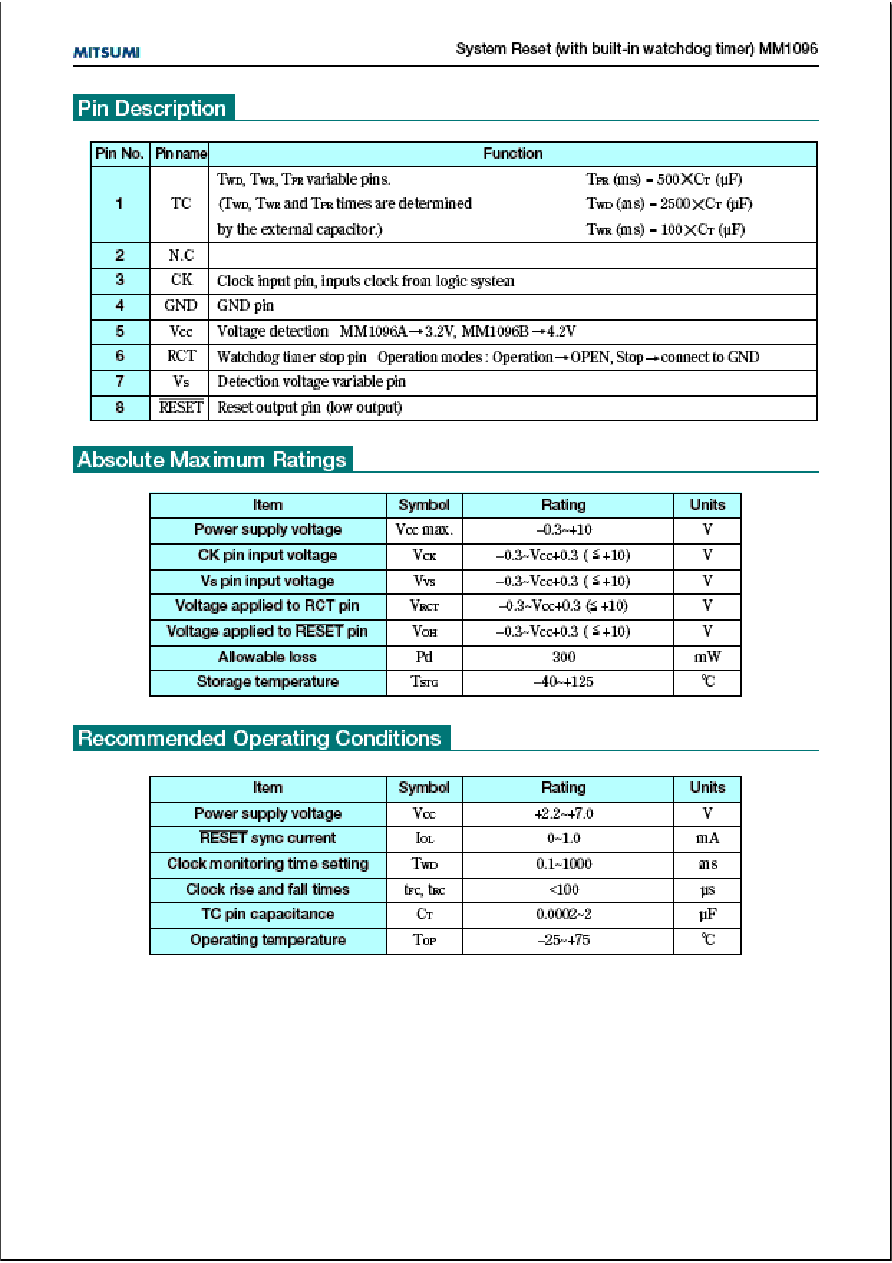
Description of Operation