MITSUMI
Compander IC MM1102
Compander IC
Monolithic IC MM1102
Features
This IC was developed for use in cordless telephones. It is a compander IC incorporating
compressor/expander circuits for a significant noise reduction effect without complicated external circuitry.
On the transmission side, the dynamic range of audio signals is compressed by the compressor circuit; on the
receiving side, the expander expands the signals. As a result the dynamic range over the transmission
channel is reduced logarithmically by one-half.
1. Can be driven at low voltages (down to 2.4V)
2. Internal mute function
3. Internal limiter (IDC) function
4. Two internal op-amps (for splatter filter)
5. Internal standby function
6. Data input, output pins
7. Independent mute circuit
Package
SSOP-24A (MM1102XF)
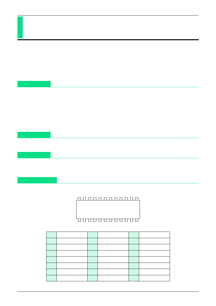
Pin Assignment
SSOP-24A
1
3
6
9
2
4 5
8
7
10
12
11
24
20
17
23
21
19 18
16
22
13
14
15
Applications
1. Cordless telephones
2. Various mobile communication devices
1
C.Vref
9
C.OUT
17
E.MUTE SW
2
C.IN
10
BUFIN 1
18
E.OUT
3
C.IN-
11
BUFOUT 1
19
E.RECT
4
C.RECT
12
GND
20
A.OUT
5
C.RIN
13
BUFIN 2
21
A.IN-
6
C.FB
14
BUFOUT 2
22
A.IN+
7
C.NF
15
STANDBY SW
23
E.Vref
8
DATA IN
16
C.MUTE SW
24
V
CC

MITSUMI
Compander IC MM1102
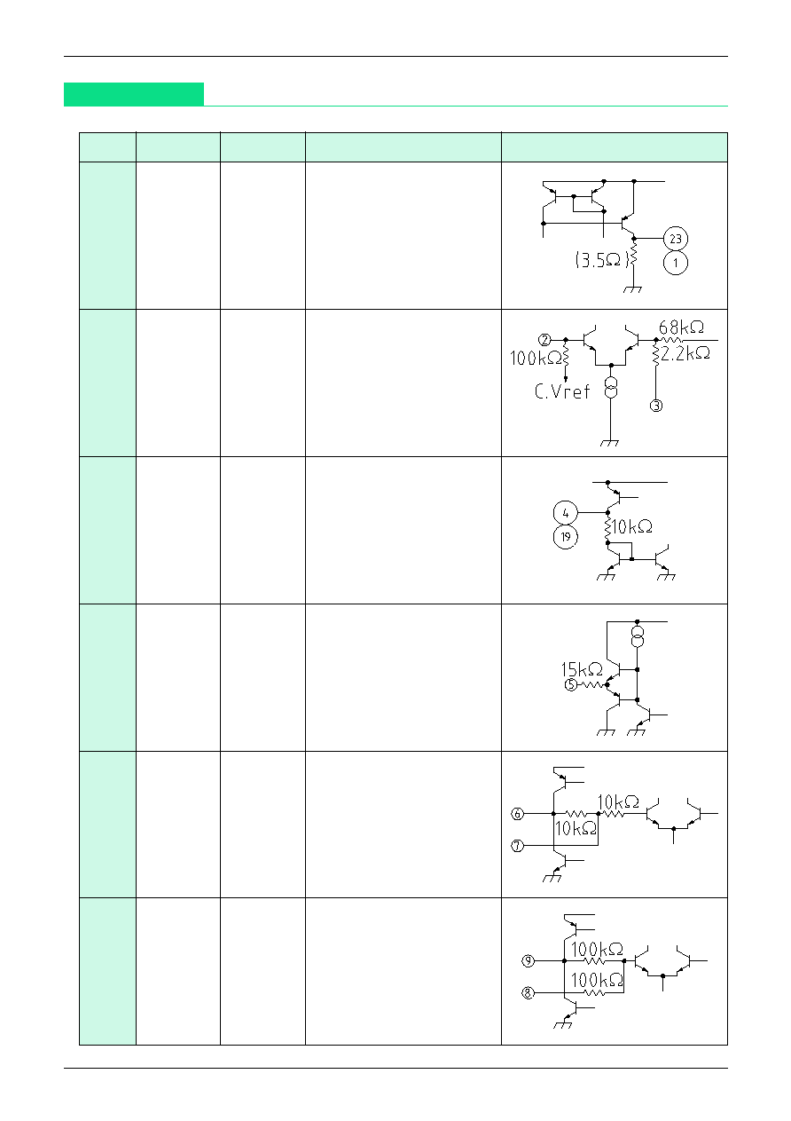
10
-
-
(13)
11
-
-
(14)
Buffer amp unit
Pin 10 (13): Input pin not
biased internally
Pin 11 (14): Output pin
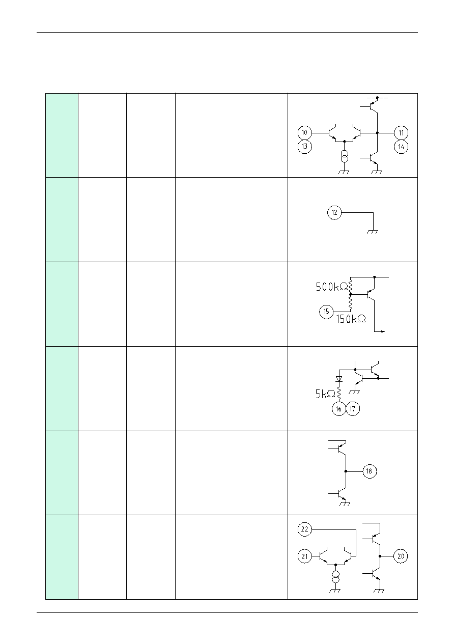
12
0V
GND pin
15
Vcc
150k
(3V)
Standby SW
The IC operates at approx.
V
CC
-1 V and below. At open
and high (V
CC
) levels, it is
in the standby state.
16
0.7V
-
17
0.7V
-
Compressor � expander
Mute SW
Muted at approx. 0.6V and
below; operates normally at
open and high levels
18
1.3V
-
Expander unit
Output pin
20
-
-
21
-
-
22
-
-
Pin 20: Output pin
Input amp
Pin 22: Input pin (+)
Pin 21: Input pin (-)
None of these are biased
internally

MITSUMI
Compander IC MM1102
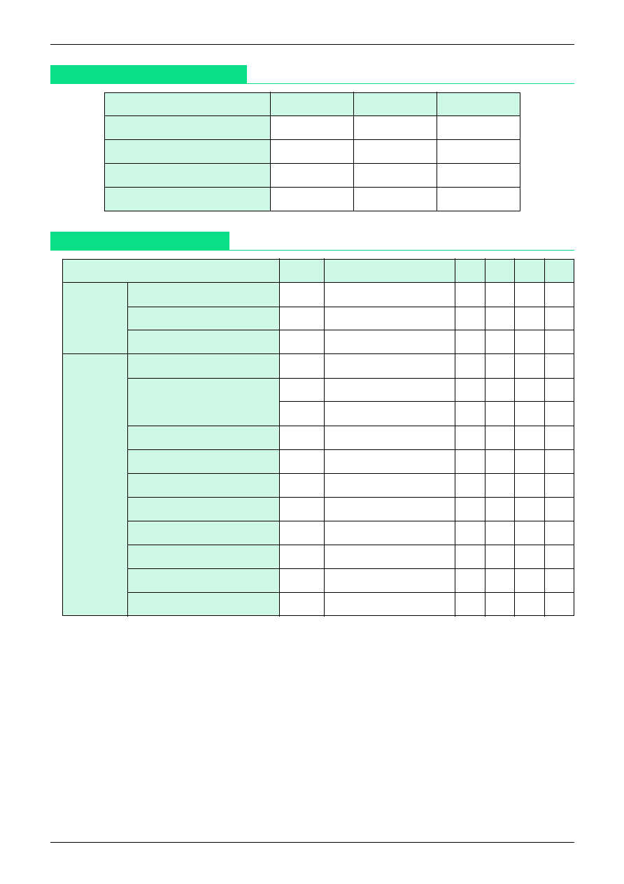
Absolute Maximum Ratings
(Ta=25
�
C)
Electrical Characteristics
(Except where noted otherwise, Ta=25
�
C, V
CC
=3V, f
IN
=1kHz)
Item
Symbol
Ratings
Units
Storage temperature
T
STG
-40~+125
�
C
Operating temperature
T
OPR
-10~+70
�
C
Power supply current
V
CC
max.
+2.4~+8
V
Allowable loss
Pd 450 mW
Item
Symbol
Measurement conditions
Min. Typ. Max. Units
Consumption current
I
CC
No signal
4.4
6.5
mA
Standby current consumption
Is
CC
0
10
�A
Threshold voltage
Vth
0.65
V
Input reference level
Vinc
V
OC
=100mVrms, V
IN
=0dB
8.0
13.5
18.0 mVrms
Gain error difference
*
Gc1
V
IN
=-20dB
-0.5
0
0.5
dB
Gc2
V
IN
=-40dB
-1.0
0
1.0
dB
Distortion
THD
C
V
IN
=0dB
0.3
1.0
%
Output noise voltage
Vnc
No signal (CCITT)
2.5
5.0
mVrms
Mute attenuation
Attc
V
IN
=0dB, Mute SW : on
-50
-40
dB
Limit voltage
Vlimc
THD=10%
1.15
1.3
1.45
V
P-P
DATA pin voltage gain
G
DATA
V
IN
=0dB, Mute SW : on
-0.5
0
0.5
dB
DATA pin maximum output
VD max.
THD=10%, Mute SW : on
0.70
Vrms
Crosstalk
CT
C
EXPV
IN
=0dB
-33
-28
dB
Ripple rejection ratio
RR
C
V
R
=100mVrms, f
R
=1kH
Z
-23
-18
dB
Compressor
unit
