MITSUMI
2-Input 1-Output Video Switch / 3-Input 1-Output Video Switch MM1111~MM1118
2-Input 1-Output Video Switch / 3-Input 1-Output Video Switch
Monolithic IC MM1111~MM1118
Outline
These ICs are video switches for video / audio signal switching, with 2-input 1-output or 3-input 1-output. The
series includes those with and without built-in clamp and 6dB amp circuits.
Circuit configuration tables and block diagrams are as follows.
MM1118 is used as the representative model in this description.
MM1111~MM1118 Series Circuit Configuration Table
MM1111~MM1118 Input/Output Voltage Measurement Values (typ.)
Model name
# of Inputs
# of Outputs
6dB amplifier
Clamp circuit
Power supply voltage
MM1111
2
1
No
No
4.6~13.0V
MM1112
2
1
Yes
No
8.0~13.0V
MM1113
3
1
No
No
4.6~13.0V
MM1114
3
1
Yes
No
8.0~13.0V
MM1115
2
1
No
Yes
4.6~13.0V
MM1116
2
1
Yes
Yes
4.6~13.0V
MM1117
3
1
No
Yes
4.6~13.0V
MM1118
3
1
Yes
Yes
4.6~13.0V
Model name
Input / Output
Power supply voltage
Unit
voltage
5V
9V
12V
MM1111
Input voltage
2.77
5.02
6.71
V
Output voltage
2.01
4.26
5.96
V
MM1112
Input voltage
4.06
5.45
V
Output voltage
4.30
5.57
V
MM1113
Input voltage
2.77
5.02
6.71
V
Output voltage
2.01
4.26
5.96
V
MM1114
Input voltage
4.06
5.45
V
Output voltage
4.30
5.57
V
MM1115
Input voltage
1.35
2.40
3.20
V
Output voltage
0.59
1.65
2.45
V
MM1116
Input voltage
1.29
2.30
3.05
V
Output voltage
1.06
1.76
2.30
V
MM1117
Input voltage
1.35
2.40
3.20
V
Output voltage
0.59
1.65
2.45
V
MM1118
Input voltage
1.29
2.30
3.05
V
Output voltage
1.06
1.76
2.30
V
MITSUMI
2-Input 1-Output Video Switch / 3-Input 1-Output Video Switch MM1111~MM1118
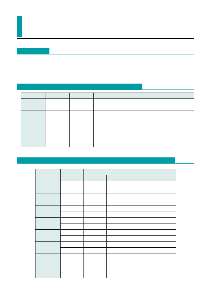
Buffer
B
i
a
s
Buffer
Bias
SW
OUT
L
IN1
H
IN2
Control input truth table
MM1111
B
i
a
s
Bias
MM1112
SW
OUT
L
IN1
H
IN2
Control input truth table
MITSUMI
2-Input 1-Output Video Switch / 3-Input 1-Output Video Switch MM1111~MM1118
Buffer
B
i
a
s
Buffer
Bias
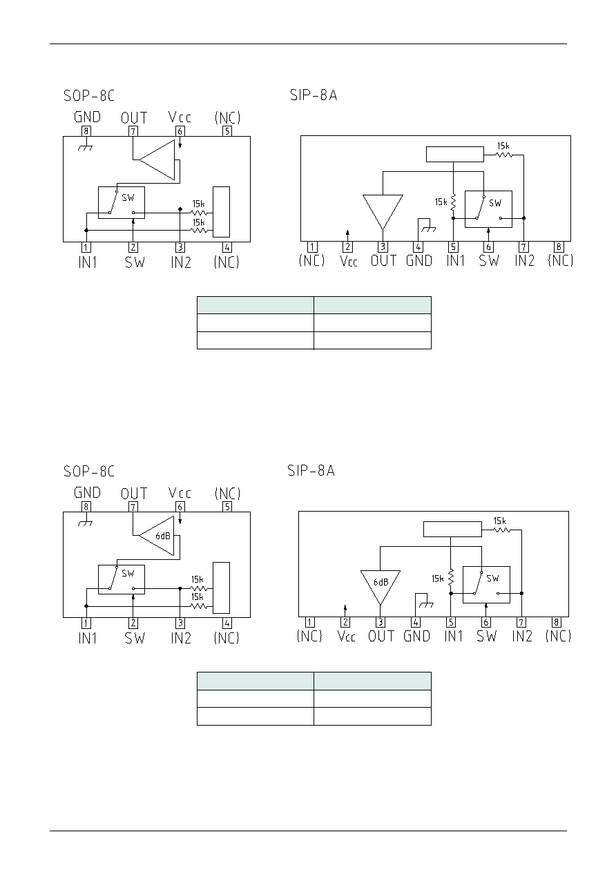
MM1113
B
i
a
s
Bias
MM1114
Control input truth table
SW1
SW2
OUT
L
L
IN1
H
L
IN2
-
H
IN3
SW1
SW2
OUT
L
L
IN1
H
L
IN2
-
H
IN3
Control input truth table

MITSUMI
2-Input 1-Output Video Switch / 3-Input 1-Output Video Switch MM1111~MM1118
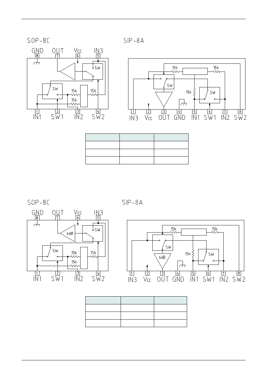
Buffer
Clamp
Clamp
B
i
a
s
Buffer
Clamp
Clamp
Bias
MM1115
Clamp
Clamp
B
i
a
s
Clamp
Clamp
Bias
MM1116
Control input truth table
SW
OUT
L
IN1
H
IN2
Control input truth table
SW
OUT
L
IN1
H
IN2
MITSUMI
2-Input 1-Output Video Switch / 3-Input 1-Output Video Switch MM1111~MM1118
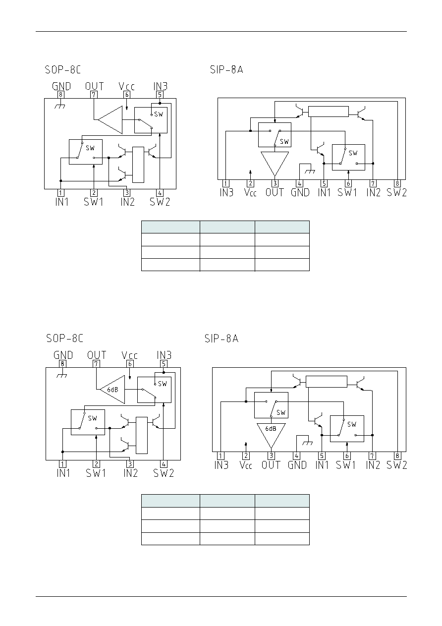
Buffer
Clamp
Clamp
Clamp
B
i
a
s
Buffer
Clamp
Clamp
Clamp
Bias
MM1117
Clamp
Clamp
Clamp
B
i
a
s
Clamp
Clamp
Clamp
Bias
MM1118
Control input truth table
SW1
SW2
OUT
L
L
IN1
H
L
IN2
-
H
IN3
Control input truth table
SW1
SW2
OUT
L
L
IN1
H
L
IN2
-
H
IN3

MITSUMI
2-Input 1-Output Video Switch / 3-Input 1-Output Video Switch MM1111~MM1118
3-Input 1-Output Video Switch (with 6dB amp)
Monolithic IC MM1118
Outline
This is a 3-input, 1-output video switch IC with a clamp function and built-in 6dB amp, for video signal
switching. One of the inputs also has a mute function.
Features
1. Built-in 6dB amp
2. Clamp function
3. Mute function
4. Current consumption
5.1mA typ.
5. Operating power supply voltage range
4.6~13.0V
6. Frequency response
10MHz
7. Crosstalk
64dB (at 4.43MHz)
Package
SOP-8C (MM1118XF)
SIP-8A (MM1118XS)
Applications
1. TV
2. VCR
3. Other video equipment
Introduction of Main Model
MITSUMI
2-Input 1-Output Video Switch / 3-Input 1-Output Video Switch MM1111~MM1118
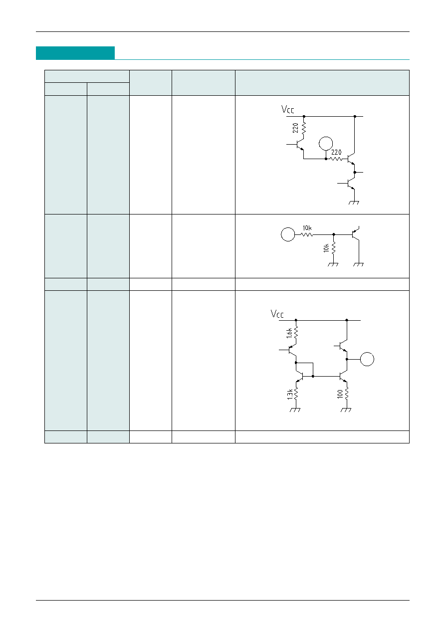
Pin Description
Pin no.
SOP-8C
SIP-8A
Pin name
Function
Internal equivalent circuit diagram
1
5
IN1
Input 1
3
7
IN2
Input 2
5
1
IN3
Input 3
2
6
SW1
Switch 1
4
8
SW2
Switch 2
6
2
V
CC
Power supply
8
4
GND
Ground
7
3
OUT
Output
MITSUMI
2-Input 1-Output Video Switch / 3-Input 1-Output Video Switch MM1111~MM1118
Absolute Maximum Ratings
(Ta=25�C)
Electrical Characteristics
(Except where noted otherwise, Ta=25�C, V
CC
=5.0V)
Item
Symbol
Ratings
Units
Storage temperature
T
STG
-40~+125
�C
Operating temperature
T
OPR
-20~+75
�C
Power supply voltage
V
CC
15
V
Allowable loss
Pd
300 (SOP-8C)
1000 (SIP-8A)
mW
Item
Symbol
Measurement conditions
Min. Typ. Max. Units
Operating power supply voltage range
V
CC
4.6
13.0
V
Consumption current
Id
Refer to Measuring Circuit
5.1
6.6
mA
Voltage gain
Gv
Refer to Measuring Circuit
5.5
6.0
6.5
dB
Frequency characteristic
F
C
Refer to Measuring Circuit
-1
0
+1
dB
Differential gain
DG
Refer to Measuring Circuit
0
�3
%
Differential phase
DP
Refer to Measuring Circuit
0
�3
deg
Output offset voltage
Voff
Refer to Measuring Circuit
�30
mV
Crosstalk
C
T
Refer to Measuring Circuit
-64
-54
dB
Switch 1 input voltage H
VIH1
Refer to Measuring Circuit
2.1
V
Switch 1 input voltage L
VIL1
Refer to Measuring Circuit
0.7
V
Switch 2 input voltage H
VIH2
Refer to Measuring Circuit
2.1
V
Switch 2 input voltage L
VIL2
Refer to Measuring Circuit
0.7
V
Output impedance
Ro
25

MITSUMI
2-Input 1-Output Video Switch / 3-Input 1-Output Video Switch MM1111~MM1118
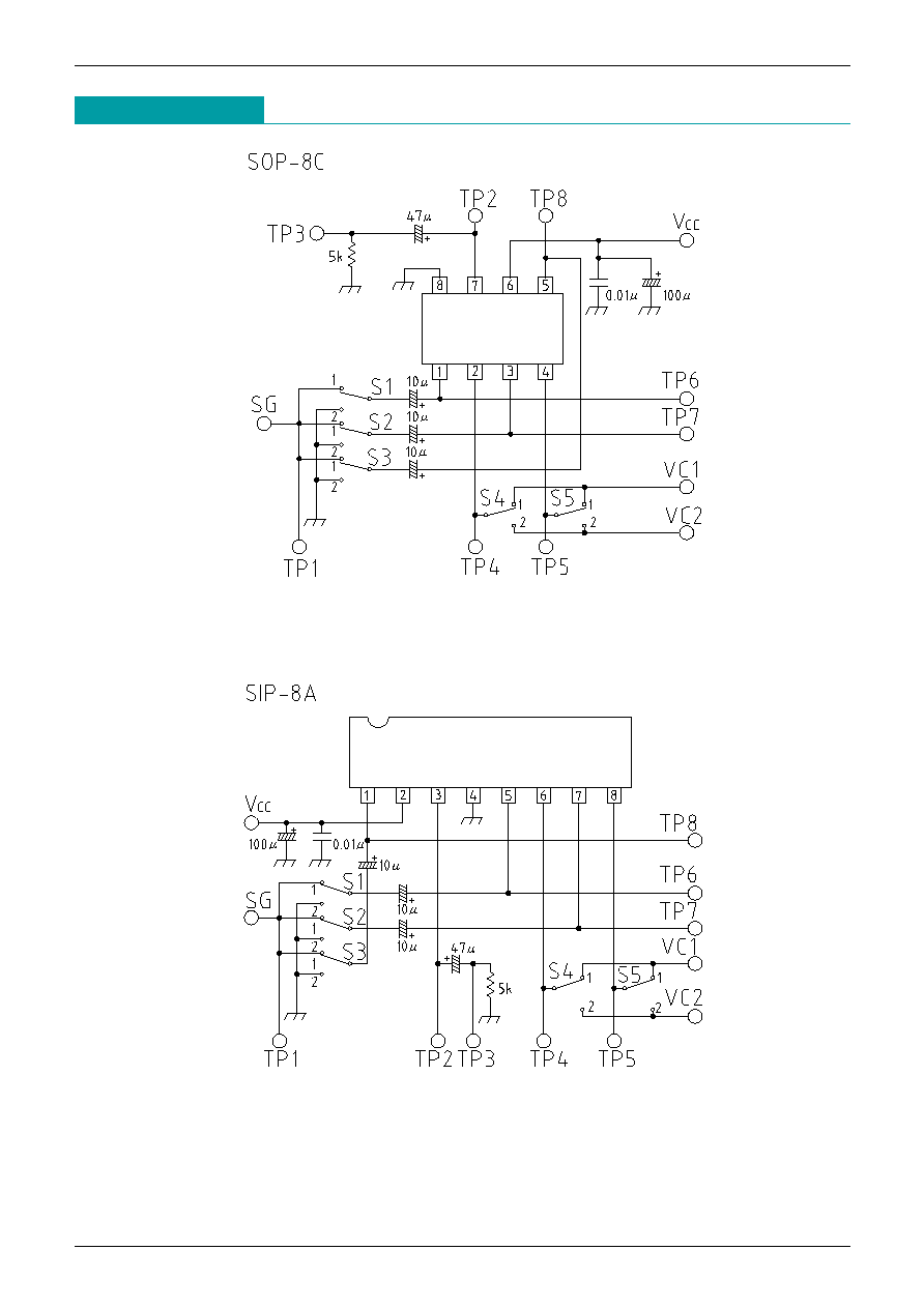
Measuring Procedures
(Except where noted otherwise, V
CC
=5.0V, VC1=V
CC
, VC2=0V)
Item
Symbol
Switch state
Measuring Procedure
S1
S2
S3
S4
S5
Consumption
Id
2
2
2
2
2
current
1
2
2
2
2
Voltage gain
G
V
2
1
2
1
2
2
2
1
1
1
2
2
1
2
1
1
2
2
2
2
Frequency
F
C
2
1
2
1
2
characteristic
2
2
1
1
1
2
2
1
2
1
1
2
2
2
2
Differential gain
DG
2
1
2
1
2
2
2
1
1
1
2
2
1
2
1
1
2
2
2
2
Differential phase
DP
2
1
2
1
2
2
2
1
1
1
2
2
1
2
1
Output offset
2
2
2
2
2
voltage
Voff
2
2
2
1
2
2
2
2
1
1
1
2
2
1
2
1
2
2
2
1
1
2
2
1
1
Crosstalk
C
T
2
1
2
2
2
2
1
2
2
1
2
1
2
1
1
2
2
1
2
2
2
2
1
1
2
Switch 1 input
2
2
2
1
2
voltage H
V
IH
1
Switch 1 input
voltage L
V
IL
1
Switch 2 input
2
2
2
2
1
voltage H
V
IH
2
Switch 2 input
voltage L
V
IL
2
Connect a DC ammeter to the V
CC
pin and measure. The
ammeter is shorted for use in subsequent measurements.
Input a 1.0V
P-P
, 100kHz sine wave to SG, and obtain G
V
from the following formula given TP1 voltage as V1
and TP3 voltage as V2.
G
V
=20LOG (V2/V1) dB
For the above G
V
measurement, given TP3 voltage for
10MHz as V3, F
C
is obtained from the following
formula.
F
C
=20LOG (V3/V2) dB
Input a 1.0V
P-P
staircase wave to SG, and measure
differential gain at TP3.
APL=10~90%
Proceed as for DG, and measure differential phase.
Measure the DC voltage difference of each switch
status at TP2.
Assume VC1=2.1V, VC2=0.7V.
Input a 2.0V
P-P,
4.43MHz sine wave to SG, and given
TP1 voltage as V4 and TP3 voltage as V5, C
T
is
obtained from the following formula.
C
T
= 20LOG (V5/V4) dB
Impress an optional DC voltage on TP6 and TP7.
Gradually raise from VC1=0V. TP4 voltage when TP7
voltage is output on TP2 is V
IH
1. Gradually lower from
VC1=V
CC
. TP4 voltage when TP6 voltage is output on
TP2 is V
IL
1.
Impress an optional DC voltage on TP6 and TP8.
Gradually raise from VC1=0V. TP5 voltage when TP8
voltage is output on TP2 is V
IH
2. Gradually lower from
VC1=V
CC
. TP5 voltage when TP6 voltage is output on
TP2 is V
IL
2.
MITSUMI
2-Input 1-Output Video Switch / 3-Input 1-Output Video Switch MM1111~MM1118
Measuring Circuit