 | –≠–ª–µ–∫—Ç—Ä–æ–Ω–Ω—ã–π –∫–æ–º–ø–æ–Ω–µ–Ω—Ç: MM1145BF | –°–∫–∞—á–∞—Ç—å:  PDF PDF  ZIP ZIP |
MITSUMI
System Reset (with built-in watchdog timer) MM1145
System Reset (with built-in watchdog timer)
Monolithic IC MM1145
Outline
This IC has a built-in watchdog timer, with 2 channels for a clock monitoring function that monitors the
microcomputer and outputs an intermittent reset signal if the microcomputer runs wild. Also, it has a power
supply voltage monitoring function (system reset function) which generates a reset signal if power supply
voltage is momentarily interrupted or drops, and performs power ON reset during normal power supply
recovery and when power is turned on.
Features
1. Built-in edge trigger input watchdog timer
2. 2 clock pulse monitoring
3. Power ON reset time (T
PR
) and watchdog timer monitoring time (T
WD
) can be set individually with external
elements (R, C)
4. Excellent watchdog timer monitoring time (T
WD
) precision
A type : ±20%
B type : ±30%
5. Watchdog function stop pin allows use as system reset IC
6. Accurate power supply voltage drop detection
4.2V±3.5%
7. Detection voltage has hysteresis
100mV typ. ±0.14%/∞C
8. Low reset minimum voltage
9. Low current consumption
150µA typ.
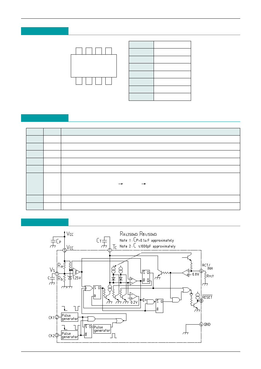
Package
SOP-8C (MM1145AF, MM1145BF)
Applications
Voltage detection for CPUs, microcomputers, etc. and clock pulse monitoring
Series Table
Model
V
SL
T
PR
T
WD
T
WR
MM1145A
4.2
100ms
50ms
10ms
MM1145B
40ms
110ms
10ms
*
C
T
=0.02µF, RC
T
=1M
V
SL
: Reset detection voltage
T
PR
: Reset hold time during Vcc rise
T
WD
: Watchdog timer monitoring time
T
WR
: Reset time
MITSUMI
System Reset (with built-in watchdog timer) MM1145
1
4
3
2
8
5
6
7
SOP-8C
(TOP VIEW)
Pin Assignment
Pin Description
Block Diagram
1
TC
2
CK1
3
CK2
4
GND
5
V
CC
6
RCT
7
V
S
8
RESET
----------------------------------------------
Pin No. Pin name
Function
1
TC
2
CK1
3
CK2
4
GND
5
V
CC
6
RCT
7
V
S
8
RESET
----------------------------------------------------------------------------------------------------------
T
WD
, T
WR
, T
PR
time setting pins. Time determined by external capacitor.
Clock input pin 1 Clock input from logic system
Clock input pin 2 Clock input from logic system
GND pin
Power supply pin Detection voltage 4.2V
Watchdog timer stop pin and T
WD
adjustment pin
Operation modes : Operation Vcc, Stop GND
T
WD
time determined by external resistor R
RCT
and C
T
Detection voltage adjustment pin
Reset output pin (low output)
MITSUMI
System Reset (with built-in watchdog timer) MM1145
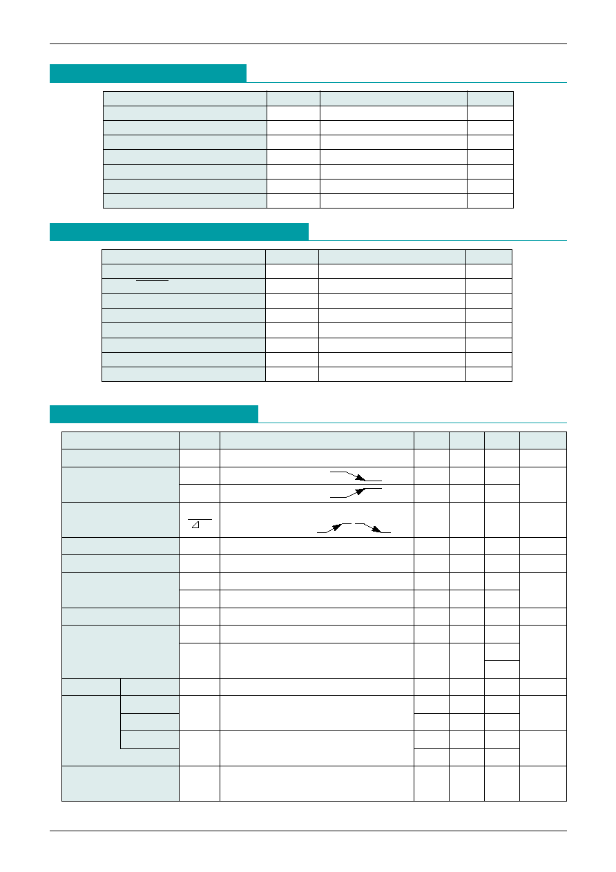
Absolute Maximum Ratings
Item
Symbol
Rating
Units
Power supply voltage
V
CC
max.
-0.3~+7.5
V
CK pin input voltage
V
CK
-0.3~V
CC
+0.3 ( <
= +7.5)
V
VS pin input voltage
V
VS
-0.3~V
CC
+0.3 ( <
= +7.5)
V
Voltage applied to RCT pin
V
RCT
-0.3~V
CC
+0.3 ( <
= +7.5)
V
Voltage applied to RESET
----------------------------------------------
pin
V
OH
-0.3~V
CC
+0.3 ( <
= +7.5)
V
Allowable loss
Pd
300
mW
Storage temperature
T
STG
-40~+125
∞
C
Recommended Operating Conditions
Item
Symbol
Rating
Units
Power supply voltage
V
CC
+2.2~+7.0
V
RESET sync current
I
OL
0~4.0
mA
Clock monitoring time setting
T
WD
1.95~10000
ms
Power supply voltage rise and fall times
t
FV
, t
RV
<300
µs
Clock rise and fall times
t
FC
, t
RC
<100
µs
C
T
pin capacitance
C
T
0.002~2
µF
RCT pin resistance
Rr
CT
0.39~2
M
Operating temperature
T
OP
-25~+75
∞
C
Item
Symbol Measurement
conditions
Min.
Typ.
Max.
Units
Consumption current
I
CC
During watchdog timer operation
150
180
µA
Detection voltage
V
SL
4.05
4.20
4.35
V
V
SH
4.15
4.30
4.45
Detection voltage
±0.01
%/
∞
C
temperature coefficient
Hysteresis voltage
V
HYS
50
100
150
mV
CK input threshold
V
TH
0.8
1.2
2
V
CK input current
I
IH
V
CK
=5.0V
0
1
µA
I
IL
V
CK
=0V
-14.5
-8.5
-4.5
Output voltage (High)
V
OH
I
=-1µA, V
S
=OPEN
4.0
4.5
V
V
OL
1
I
=0.5mA, V
S
=0V
0.10
0.20
Output voltage (Low)
V
OL
2
I
=2.0mA, V
S
=0V
0.15
0.35
V
0.30
Output sync current
I
OL
V
=1.0V, V
S
=0V
2
4
mA
MM1145A
I
CT
1
During watchdog timer operation
-0.40
-0.48
-0.60
µA
C
T
charge
MM1145B
-0.17
-0.22
-0.30
current
MM1145A
I
CT
2
During power ON reset operation
-0.21
-0.31
-0.62
µA
MM1145B
-0.62
-0.93
-2.33
Minimum operating power supply
V
CCL
0.8
1.0
V
voltage to ensure RESET
-----------------------------------------------
RESET
--------------------------------------------
RESET
--------------------------------------------
RESET
--------------------------------------------
RESET
--------------------------------------------
V
S
=OPEN, V
CC
V
S
=OPEN, V
CC
V
SH
-V
SL
, V
CC
V
=0.4V
I
=0.1mA
RESET
--------------------------------------------
RESET
--------------------------------------------
VS
T
Electrical Characteristics (DC)
(Except where noted otherwise, Ta=25∞C, Vcc=5.0V)
MITSUMI
System Reset (with built-in watchdog timer) MM1145
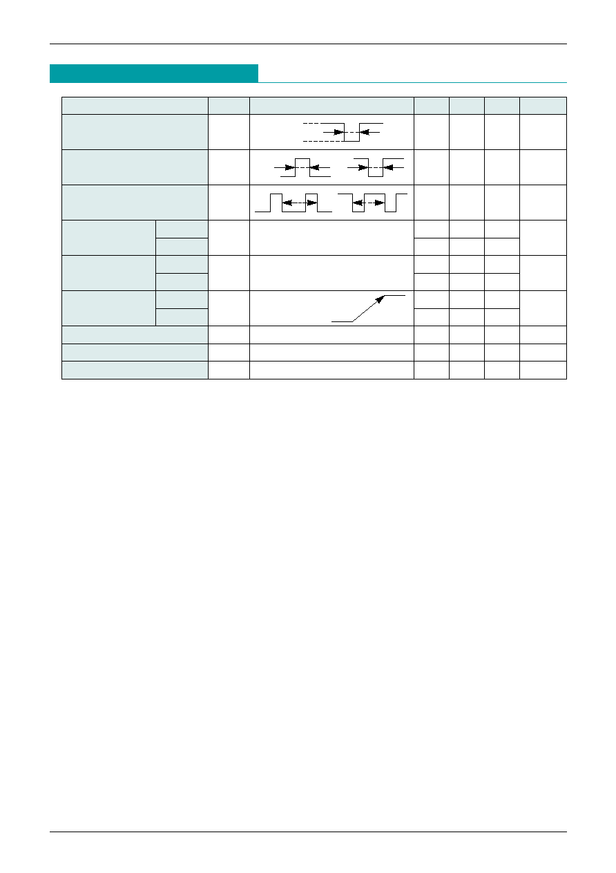
Electrical Characteristics (DC)
(Except where noted otherwise, Ta=25∞C, V
CC
=5.0V)
(Except where noted otherwise, resistance unit is
)
Item
Symbol Measurement
conditions
Min.
Typ.
Max.
Units
V
CC
input pulse width
T
PI
8
µs
CK input pulse width
T
CKW
1
T
CKW
2
3
µs
CK input cycle
*
7
T
CK
1
T
CK
2
200
µs
Watchdog timer
MM1145A
T
WD
C
T
=0.02µF, R
RCT
=1M
40
50
60
ms
monitoring time
*
1 MM1145B
80
110
140
Watchdog timer
MM1145A
T
WR
C
T
=0.02µF, R
RCT
=1M
5
10
15
ms
reset time
*
2
MM1145B
5
10
15
Reset hold time for MM1145A
T
PR
50
100
150
ms
power supply rise
*
3 MM1145B
20
40
60
Output delay time from V
CC
*
4
T
PD
RESET
--------------------------------------------------------------------------------------
pin, R
L
=10k, C
L
=20pF
2
10
µs
Output rise time
*
5
t
R
RESET
--------------------------------------------------------------------------------------
pin, R
L
=10k, C
L
=20pF
2.0
4.0
µs
Output fall time
*
5
t
F
RESET
--------------------------------------------------------------------------------------
pin, R
L
=10k, C
L
=20pF
0.2
1.0
µs
V
CC
5.0V
4.0V
CK
or
C
T
=0.02µF
R
RCT
=1M
or
Notes:
*
1 Monitoring time is the time from the last pulse (negative edge) of the timer clear clock pulse until reset
pulse output.
In other words, reset output is output if a clock pulse is not input during this time.
*
2 Reset time means reset pulse width. However, this does not apply to power ON reset.
*
3 Reset hold time is the time from when V
CC
exceeds detection voltage (V
SHR
) during power ON reset until
reset release (RESET
------------------------------------------------
output high).
*
4 Output delay time is the time from when power supply voltage drops below detection voltage (V
SL
) until
reset state occurs (RESET
------------------------------------------------
output low).
*
5 The voltage range when measuring output rise and fall time is 10~90%.
*
7 1 Set CK1 and CK2 input cycles within the following range.
T
CK
1 <
= nT
CK
2<T
WD
(ms) (n <
= 1)
RESET
------------------------------------------------
output may go low even if CK1 and CK2 are input without these conditions being met.
(Recommended use is for T
CK
1 <
= nT
CK
2)
2 T
CK
1, T
CK
2 <
= 200 µs results in the following operation.
Discharge switches to charging with the CK2 pulse (negative edge) that inputs 200µs after C
T
switches
from charging to discharge by the CK2 pulse (negative edge). RESET
------------------------------------------------
output stays high while this
operation is being repeated. (However, T
CK
1, T
CK
2 >
= 20µs.)
V
CC
MITSUMI
System Reset (with built-in watchdog timer) MM1145
Formula for C
T
Pin External Constant
Watchdog timer monitoring time (T
WD
), watchdog timer reset time (T
WR
) and reset hold time (T
PR
) during power
supply rise can be changed by varying C
T
capacitance. T
WD
also can be changed with R
RCT
.
The variable times are expressed by the following.
1. MM1145A
2. MM1145B
T
PR
(ms)
.
=. 5000 C
T
(µF)
T
PR
(ms)
.
=. 2000 C
T
(µF)
T
WD
(ms)
.
=. 2500 C
T
(µF)
R
RCT
(M
)
T
WD
(ms)
.
=. 5500 C
T
(µF) R
RCT
(M
)
T
WR
(ms)
.
=. 500 C
T
(µF)
T
WR
(ms)
.
=. 500 C
T
(µF)
Example : when C
T
=0.02µF, R
RCT
=1M
Example : when C
T
=0.02µF, R
RCT
=1M
T
PR
.
=. 100ms
T
PR
.
=. 40ms
T
WD
.
=. 50ms
T
WD
.
=. 110ms
T
WR
.
=. 10ms
T
WR
.
=. 10ms
The ratio between T
PR
and T
WD
can be changed within the range below by adjusting T
WD
with R
RCT
.
1. MM1145A
2. MM1145B
T
WD
/T
PR
.
=. 2.0 R
RCT
(0.39 (M
) <
= R
RCT
<
= 2 (M
))
T
WD
/T
PR
.
=. 2.75 R
RCT
(0.39 (M
) <
= R
RCT
<
= 2 (M
)
Formula for Watchdog Timer Monitoring Time (T
WD
) Adjustment
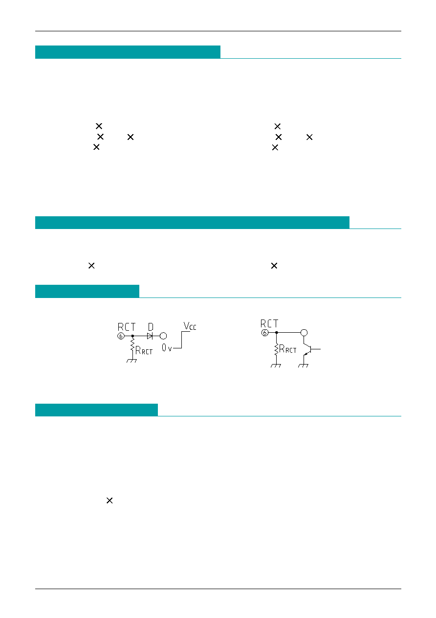
How to Use RCT Pin
Example 1
Example 2
1. Watchdog timer operates when RCT pin is open.
2. Watchdog timer stops operating when RCT pin is connected to ground.
Description of Operation
1. RESET
--------------------------------------------
goes low when V
CC
rises to approximately 0.8V.
Approximately 1µA (V
CC
=0.8V) of pull up current is output from RESET.
2. Capacitor C
T
charging starts when V
CC
rises to V
SH
(
.
=. 4.3V). Output is in reset state at this time.
3. Output reset is released (RESET
-------------------------------------------
goes high) after a certain time (T
PR
), from when C
T
starts charging until
discharge (the time from when C
T
voltage reaches a certain threshold value VT1 (
.
=. 1.4V) until C
T
voltage
drops to a certain threshold value VT2 (
.
=. 0.2V).
Reset hold time : T
PR
is as follows.
T
PR
(ms)
.
=. 5000 C
T
(µF)
C
T
charging starts again after reset release, and watchdog timer operation begins.
Clock input during power ON reset time (T
PR
) will cause mis-operation.
4. If CK1 and CK2 are input in that order (or simultaneously) during C
T
charging, CK2 negative edge trigger
causes the TC pin to switch from charging to discharge.
5. Discharge switches to charging when C
T
voltage drops to threshold value VT2 (
.
=. 0.2V). Steps 4 and 5 are
repeated while a normal clock is input from the logic system.
MITSUMI
System Reset (with built-in watchdog timer) MM1145
6. Operation is as follows if either clock CK1 or CK2 ceases (the figure shows CK1).
Output goes to reset state (RESET
-------------------------------------------
goes low) when C
T
voltage reaches reset ON threshold value VT1
(
.
=. 1.4V).
The formula for C
T
charging time (T
WD
: watchdog timer monitoring time) until reset is output is as follows.
T
WD
(ms)
.
=. 2500 C
T
(µF)
7. Watchdog timer reset time T
WR
is the discharge time until C
T
voltage drops to reset OFF threshold value
VT2 from reset ON threshold value VT1. The formula is as follows.
T
WR
(ms)
.
=. 500 C
T
(µF)
After reset OFF threshold value is reached, output reset is released and C
T
starts charging. Thereafter,
steps 4 and 5 are repeated if a normal clock is input, and when one of the clocks ceases, 6 and 7 are
repeated.
In the same way, 6 and 7 are repeated if both clocks CK1 and CK2 cease.
8. Reset is output when V
CC
drops to V
SL
(
.
=. 4.2V). C
T
is charged simultaneously.
9. C
T
charging starts when V
CC
rises to V
SH
.
When V
CC
drops momentarily, C
T
charging begins after the charge is first discharged, if the time from V
CC
dropping below V
SL
until it rises to V
SH
is longer than the V
CC
input pulse width standard value T
PI
.
10.Output reset is released after V
CC
goes above V
SH
and after T
PR
, and the watchdog timer starts.
11.Watchdog timer operation can be stopped by switching R
CT
voltage from high to low. (Clocks CK1 and
CK2 are invalid. Regardless of status, TC pin voltage discharges quickly and goes to 0V.) This operation
can be applied from any timing. In this state the IC functions as a reset IC with power ON reset.
12.Watchdog timer operation re-starts when R
CT
voltage switches to high.
13.When power is OFF, reset is output if V
CC
goes below V
SL
.
14.When Vcc drops to 0V, reset output is held until V
CC
reaches 0.8V.
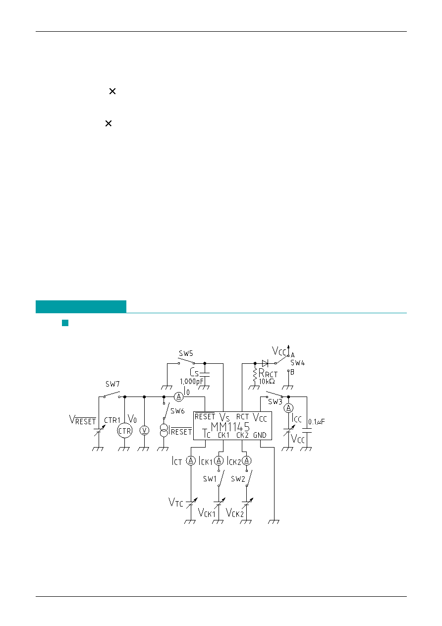
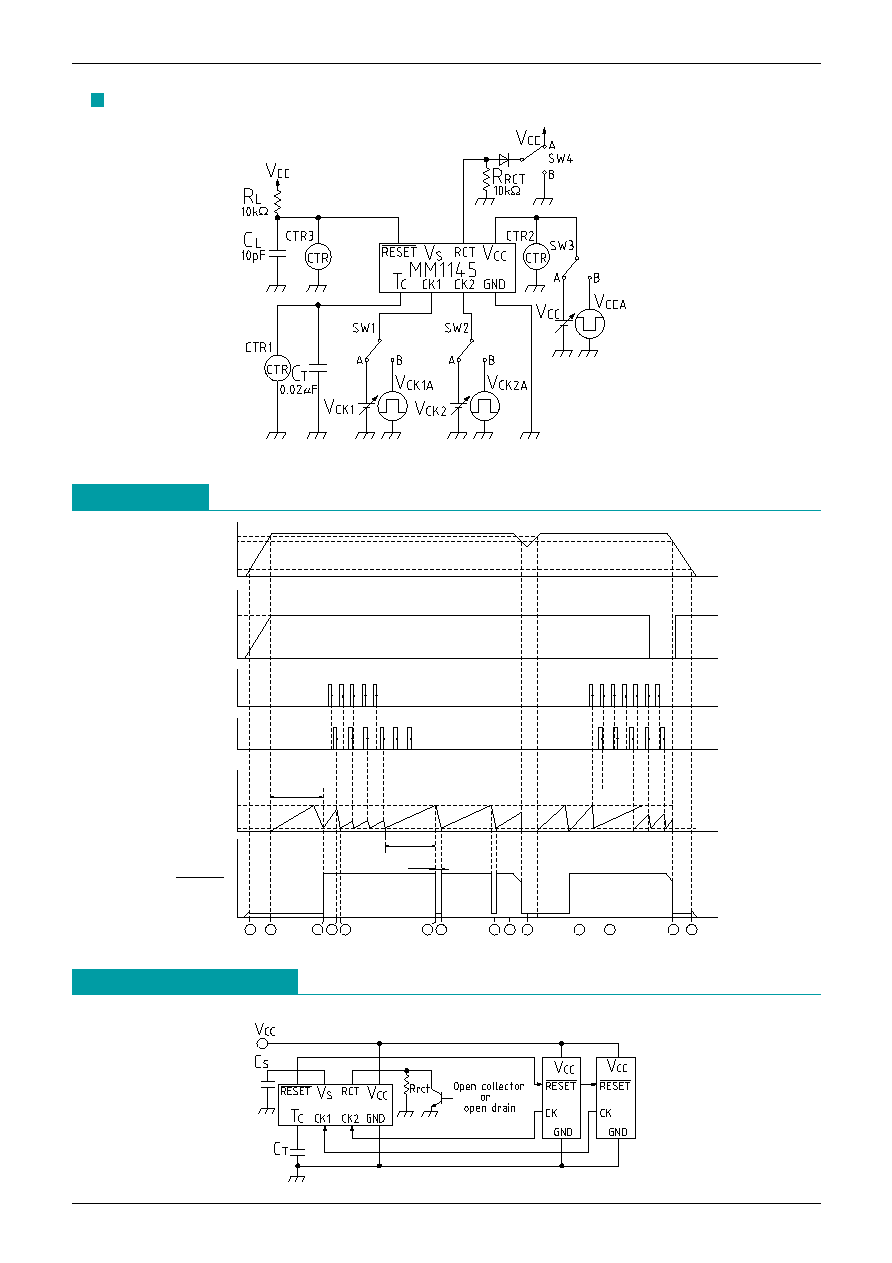
Measuring Circuit
Measuring Circuit 1
MITSUMI
System Reset (with built-in watchdog timer) MM1145
Timing Chart
V
CC
RCT
CK1
CK2
C
T
V
H
V
L
0.8
RESET
VT1
VT2
T
PR
T
WD
T
WR
1
2
3
4
5
6
7
8
9
10
11
12
13
14
Basic Circuit Diagram
Measuring Circuit 2