MITSUMI
Flame Detection Amplifier MM1217
Flame Detection Amplifier
Monolithic IC MM1217
Outline
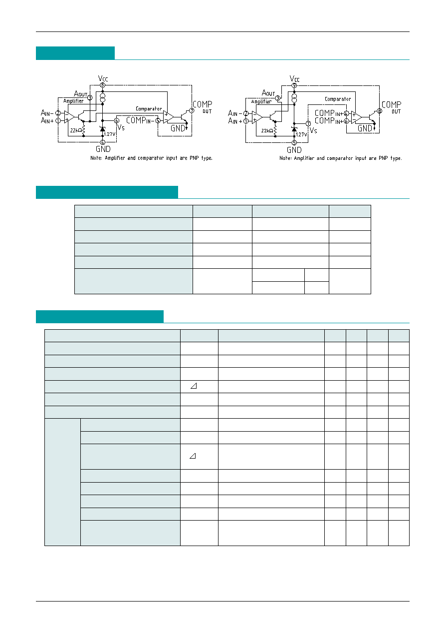
This IC is comprised of an operation amplifier, a comparator, and a reference power source. It is worthy of
note that the input offset voltage and the input offset voltage temperature drift of this operation amplifier are
one digit less than those of conventional products regardless of the single power supply. Formerly, offset
voltage adjustment was required for flame detection using a thermocouple on gas appliances, but with this IC
adjustment is not required.
Due to the single power supply, low current consumption, and low offset voltage, two batteries can be used
for operation, making it appropriate for equipment that amplifies the very small signal of portable equipment.
Features
General
1. Power supply voltage (single batteries)
V
CC
=1.8V~6V
(It is available to operate by two dry cell batteries.)
2. Current consumption
0.1mA typ.
3. Power supply line elimination ratio
60dB typ.
Amplifier section
1. Low input offset voltage
±0.1mV typ.
2. Low input offset voltage drift (-20∞C~+75∞C) ±1.0µV/∞C
typ.
3. Input offset current
1nA typ.
4. Input bias current
50nA typ.
5. Voltage gain
100dB typ.
Comparator Section
1. Input offset voltage
±1.0mV typ.
2. Low input offset voltage drift (-20∞C~+75∞C)
±10µV/∞C typ.
3. Input bias current
±25nA typ.
4. Output sink current
5mA min.
Reference Voltage Section
1. Reference voltag
1.27V±0.05V
2. Reference voltage temperature characteristics
±100ppm/∞C typ.
3. Output current
0.3mA min.
Applications
1. Gas burners
2. Instantaneous gas water heaters
Package
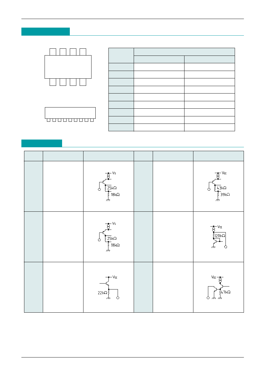
SOP-8D (MM1217XF)
SIP-9A (MM1217XS)

MITSUMI
Flame Detection Amplifier MM1217
Block Diagram
MM1217XF
MM1217XS
Absolute Maximum Ratings
(Ta=25∞C)
Item
Symbol
Specification
Units
Storage temperature
T
STG
-40~+125
∞C
Operating temperature
T
OPR
-20~+85
∞C
Power supply voltage
V
CC
max.
-0.3~+10
V
Input voltage
V
IN
-0.3~+10
V
Allowable power dissipation
Pd
MM1217XF
300
mW
MM1217XS
470
Electrical Characteristics
(Unless otherwise specified Ta=25∞C, V
CC
=3V, V
IN
=0V)
Item
Symbol
Measurement Conditions
Min. Typ. Max. Units
Current consumption
I
CC
0.1
0.15
mA
Reference voltage output current
I
OVS
1
0.3
mA
Reference voltage
V
S
1
1.22
1.27
1.32
V
Reference voltage temperature drift
V
S
1
±100
ppm/∞C
Power supply line elimination ratio
P
SRR
f=100Hz
50
60
dB
Power supply voltage range
V
CC
1.8
3.0
6.0
V
Input voltage range
V
I
-0.2
0.3
V
Input offset voltage
V
IOA
±0.1 ±0.35
mV
Input offset voltage
temperature drift
V
IOA
±1.0
±3.0
µV/∞C
Input offset current
I
IOA
1
10
nA
Input bias current
I
BA
50
150
nA
Voltage gain
G
V
R
L
=100k
80
100
dB
Output current
I
OA
V
IN
=10mV, V
O1
=0.5V
0.5
mA
Output voltage
V
OA
V
IN
=-5~25mV
V
CC
R
L
=10k
0.01
-1.0
V
Amplifier
section

MITSUMI
Flame Detection Amplifier MM1217
Electrical Characteristics
Unless otherwise specified (Ta=25∞C, V
CC
=3V, V
IN
=0V)
Note 1 : Amplifier output ∑∑∑ emitter-follower (pull-down resistance 22k
)
Note 2 : Comparator output ∑∑∑ open collector
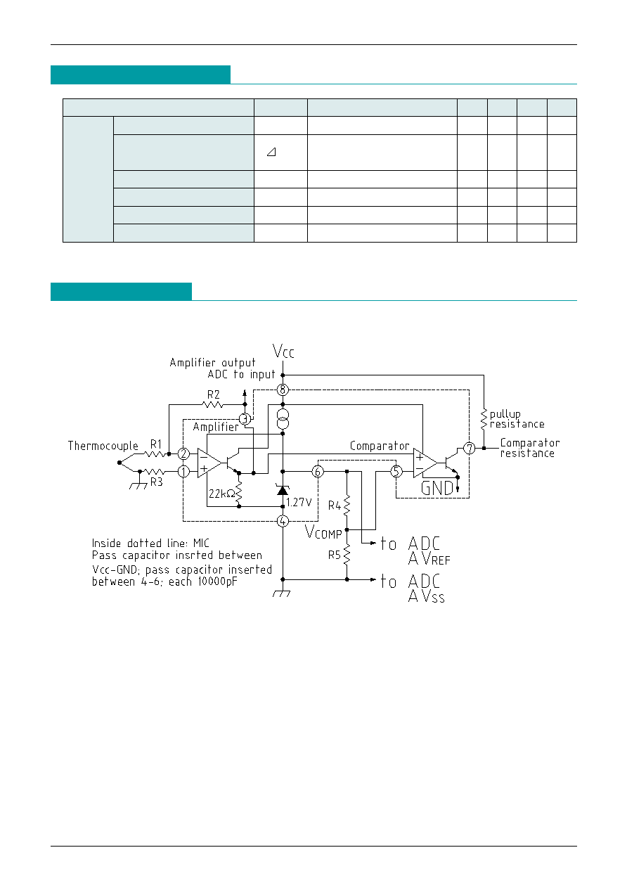
Application Circuits
Note 1: Use a gain range of 20dB-50dB in the amplifier section (40dB recommended) .
Also, insert the capacitor between output 3 and GND instead of parallel to R2 in order to eliminate noise
from the input. Please note that use of the equipment under different conditions will cause vibration.
Note 2: Applicable circuits shown are typical examples provided for reference purposes. Mitsumi cannot assume
responsibility for any problems arising out of the use of these circuits or for any infringement of third
party patent and other right due to same.
Item
Symbol
Measurement Conditions
Min. Typ. Max. Units
Input offset voltage
V
IOC
V
IN
=-5mV
±1.0
±3.5
mV
Input offset voltage
temperature drift
V
IOC
V
IN
=-5mV
±10
±30
µV/∞C
Input bias current
I
BC
V
IN
=-5mV
25
75
nA
Output sink current
I
SINK
V
IN
=10mV, V
O2
=0.4V
5
mA
Output leak current
I
LC
V
O2
=V
CC
+1V
0.2
µA
Output saturation voltage
I
SAT
V
IN
=10mV, I
SINK
=5mA
200
400
mV
Comparator
Section
Flame detection circuit using a thermocouple (single power source)

