 | –≠–ª–µ–∫—Ç—Ä–æ–Ω–Ω—ã–π –∫–æ–º–ø–æ–Ω–µ–Ω—Ç: MM1248XF | –°–∫–∞—á–∞—Ç—å:  PDF PDF  ZIP ZIP |

MITSUMI
Control of Lithium Ion Battery Charging and Discharging MM1248
Control of Lithium Ion Battery Charging and Discharging
Monolithic IC MM1248
Outline
This IC was developed for use in controlling charging and discharging of lithium ion batteries (battery modules
with three cells connected in series). In charging control, the voltage of the battery module as a whole is
controlled in constant-voltage control. Discharge control and monitoring of overvoltage rely on monitoring of
the voltages of individual cells.
Features
1. Charging control voltage
V
BATH
=12.465V±1.5% (Ta=-20∞C~70∞C)
2. Overcharge detection voltage
V
CELL
=4.335V±1.5% (Ta=-20∞C~70∞C)
3. Internal circuit for setting dead time (for overvoltage detection, discharge control)
4. Low consumption current on overdischarge
I
BATH
3=1µA typ.
5. High-precision internal overvoltage detection startup circuit (cell voltage 4.2V or higher at end of charging)
Package
SOP-16B (MM1248XF)
Absolute Maximun Ratings
(Except where noted otherwise, Ta=25∞C)
Item
Symbol
Ratings
Units
Storage temperature
T
STG
-40~+125
∞C
Operating temperature
T
OPR
-20~+70
∞C
Input voltage
V
IN
max.
18
V
Charge voltage
V
BAT
max.
15
V
Power supply voltage
V
CC
max.
15
V
Voltage applied to OV2 pin
V
O
2 max.
10
V
Allowable loss
Pd
350
mW
MITSUMI
Control of Lithium Ion Battery Charging and Discharging MM1248
Electrical Characteristics
(Except where noted otherwise, Ta=25∞C, V
IN
=15 V, C
ON
=VIN)
Item
Symbol
Measurement conditions
Min. Typ. Max. Units
Consumption current 1(pin V
IN
)
V
IN
V
IN
=15V, C
ON
=0V
250
350
µA
Consumption current (pin V
CC
) 1
I
CC
1
V
CELL
=4.4V
2.1
2.6
mA
Consumption current (pin V
CC
) 2
I
CC
2
V
CELL
=4.2V, C
ON
=0V
1.5
2.0
mA
Consumption current (pin V
CC
) 3
I
CC
3
V
CELL
=4.2V, C
ON
=V
IN
1.0
1.3
mA
Consumption current (pin V
CC
) 4
I
CC
4
V
CELL
=4.0V
50
100
µA
Consumption current (pin V
CC
) 5
I
CC
5
V
CELL
=2.4V
0.1
µA
Consumption current (pin B
ATH
) 1
I
BATH
1
V
CELL
=4.4V
5.0
10.0
µA
Consumption current (pin B
ATH
) 2
I
BATH
2
V
CELL
=4.0V
2.5
5.0
µA
Consumption current (pin B
ATH
) 3
I
BATH
3
V
CELL
=2.4V
1.0
2.0
µA
Charging control voltage
V
BATH
Ta=-20~70∞C
12.270 12.465 12.670
V
Overcharge detection voltage
V
CELL
U
Ta=-20~70∞C
4.270
4.335
4.400
V
Overcharge reset voltage
V
CELL
O
V
CELL
U V
CELL
U V
CELL
U
-60mV -45mV -30mV
V
Sensing voltage margin 1
V
UO
1
V
BATH
/3-V
CELL
U
100
mV
Sensing voltage margin 2
V
UO
2
V
BATH
-V
CELL
U 3
300
mV
Overvoltage sensing operation voltage
V
ALM
4.05
4.20
4.35
V
Overvoltage sensing hysteresis voltage
V
ALM
50
90
130
mV
Overdischarge detection voltage
V
CELL
S
2.31
2.40
2.49
V
Discharge resume voltage
V
CELL
D
2.49
2.65
2.81
V
Overdischarge sensing hysteresis voltage
V
CS
D
V
CELL
D-V
CELL
S
175
250
325
mV
Pin 11 input current 1
I11
V
CELL
=4.0V
100
200
300
nA
Pin 11 input current 2
I11A
V
CELL
=4.4V
0.7
1.0
1.3
µA
Pin 13 input current 1
I13
V
CELL
=4.0V
100
200
300
nA
Pin 13 input current 2
I13A
V
CELL
=4.4V
0.7
1.0
1.3
µA
Pin 14 input current
I14
V
CELL
=4.0V
7.7
10.0
14.3
µA
CON pin threshold voltage
V
TH
C
ON
V
IN
-1.8
V
IN
-0.4
V
CON pin input current
I
IN
C
ON
V
IN
-C
ON
=1.8V
100
µA
CON pin leakage current
I
L
C
ON
V
IN
-C
ON
=0.4V
1.0
µA
CHG pin pull-up resistance
R
CHG
Resistance across pins V
IN
and C
HG
14
20
26
k
CHG pin sync current
IS
CGH
V
BATT
<12V
100
µA
CHG pin output voltage L
V
TH
C
H
L
V
IN
-C
HG
, I
CGH
=20µA
6.2
V
CHG pin output voltage H
V
TH
C
H
H
V
IN
-C
HG
, I
CGH
=20µA
0.4
V
DCHG pin source current
I
SO
D
CH
20
µA
DCHG pin sync current
I
SI
D
CH
20
µA
DCHG pin output voltage L
V
TH
D
C
L
B
ATH
-D
CHG
, IS=20µA
1.0
V
DCHG pin output voltage H
V
TH
D
C
H
D
CHG
-G
ND
, IS=-20µA
0.8
V
OV2 pin sync current
I
SO
O
V
2
100
µA
OV1 pin source current
I
SO
O
V
1
100
µA
OV1 pin pulldown resistance
RO
V
1
35
50
65
k
CCC pin charge current
IC
CC
V
CELL
=4.4V, C
CC
=3.0V
150
220
290
nA
CCC pin threshold voltage
V
TH
C
CC
C
CC
=0V 5V
4.10
4.30
4.50
V
CCC initialization delay time
TI
NT
C
CC
=0.068µF
10
mS
CDC pin charge current
IC
DC
V
CELL
=2.8V, C
CC
=3.0V
260
380
500
nA
CDC pin threshold voltage
V
TH
C
DC
C
CC
=0V 5V
4.20
4.40
4.60
VC
Overvoltage sensing dead time
TDC
CC
C
CC
=0.068µF
0.5
1.0
1.5
S
Overdischarge sensing dead time
TDC
DC
1
C
DC
=0.1µF
0.5
1.0
1.5
S
Overdischarge reset dead time
TDC
DC
2
C
DC
=0.1µF
0.5
1.0
1.5
S
Battery voltage monitor output
VB
MON
-1.0
0
1.0
%
voltage ratio
Battery voltage monitor output current
IL
MON
50
µA
(B
ATH
-GND) ˜3
V
BATT
MITSUMI
Control of Lithium Ion Battery Charging and Discharging MM1248
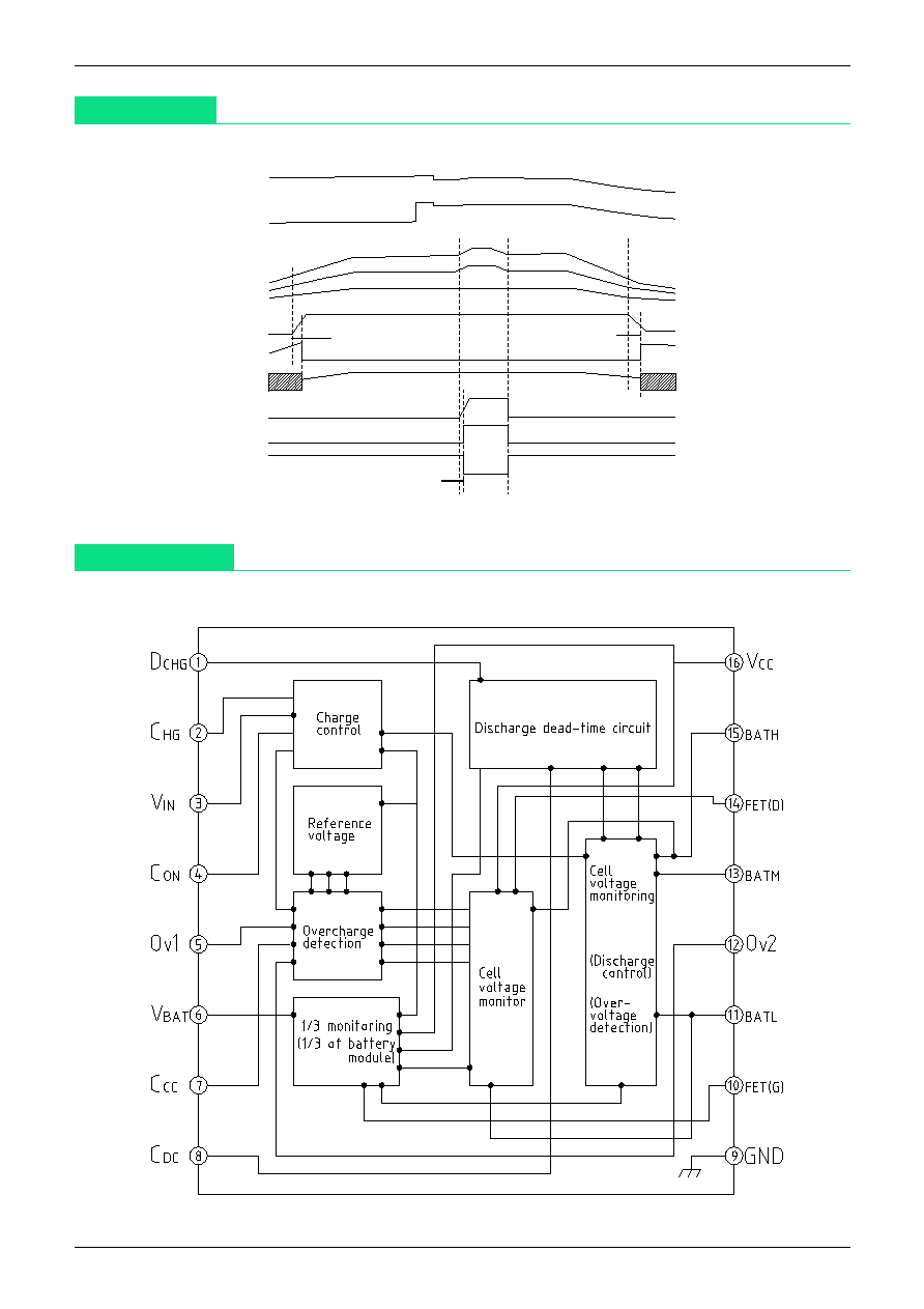
Timing Chart
V
IN
C
ON
B
ATH
B
ATL
C
DC
D
CHG
V
BAT
O
V2
C
CC
O
V1
B
ATM
tDC
DC1
tDC
CC
tDC
DC2
Unsettled
Unsettled
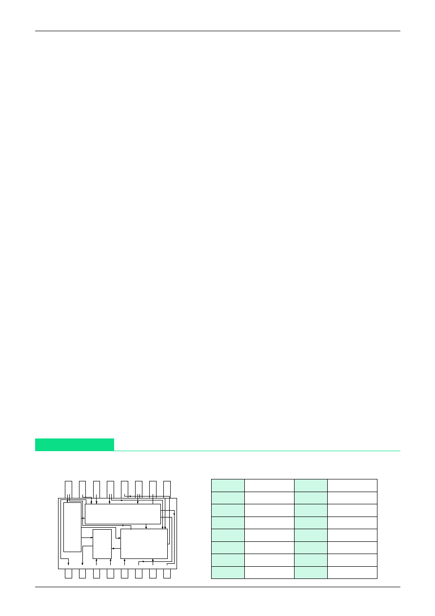
Block Diagram

MITSUMI
Control of Lithium Ion Battery Charging and Discharging MM1248
Application Circuits

MITSUMI
Control of Lithium Ion Battery Charging and Discharging MM1248
Circuit conventions
∑ Charge control unit
∑ Overcharge detection unit
Subtraction amp, buffer amp, voltage comparator, dead time setting circuit
∑ Discharge control unit
Cell voltage monitoring circuit, dead time setting circuit
∑ Overvoltage sensing (rough detection) unit
∑ High-precision reference voltage unit
Operating outline
1. Charge control
Charge control is turned on and off using the CON pin; when CON is low the charge control unit is in
operation. The error amp of the charge control unit takes inputs of 4.155V from the high-precision reference
voltage unit and the battery module voltage monitor output. The battery module voltage monitor outputs a
voltage equal to 1/3 the battery module voltage, so that in charging control the charging control FET (pin 2)
is controlled such that the battery module voltage is 4.155 3 V.
This block performs constant-voltage control only; current limiting (constant-current control) should be
implemented on the charging input side.
2. Overcharge detection
There are two blocks for overcharge detection; three output modes are provided according to input
conditions and cell voltage.
1. Charging signal on (during discharge)
2. Charging signal off (during discharge)
3. Discharge off
2-1. Charging signal on
The high-precision overcharge sensing unit is always in the operating state, and the voltage of each cell is
monitored.
In order to monitor each cell's voltage precisely, subtraction amps are provided for monitoring M and H cell
voltages, and a buffer amp is used to monitor the L cell voltage. By means of these amps the voltage of
each cell is converted to a GND-reference voltage, and compared with the high-precision reference voltage
of 4.335V.
If the voltage of any one of the cells exceeds 4.335V, the overvoltage is sensed, and the dead time setting
pin (CCC pin 7) is charged by a constant current; when the CCC pin is charged to the threshold voltage of
the dead time setting circuit (4.35V), an overvoltage signal is output.
(OV1 pin "H", OV2 pin "L")
When an overcharge signal is output, the overvoltage monitoring unit switches from the overvoltage state
to the reset monitoring state, and an overcharge signal is output until the voltages of all cells fall to 4.16 V.
To summarize the sequence of operations, when the voltage of any of the cells remains in the overcharge
state continuously for the specified time (the dead time), that cell is judged to be in an overcharged state
and is switched to overvoltage output; when all the cell voltages drop to the overcharge reset voltage or
below, the overcharge state is canceled.
On entering the overcharge state, if the charge control unit circuit is turned off, the latter unit will not
operate.
Pin
Output logic
Output type
Normal
Overvoltage
OV1
L
H
PNP output, internal pull-down resistance
OV2
High impedance
L
NPN open-collector output
MITSUMI
Control of Lithium Ion Battery Charging and Discharging MM1248
2.2. Charging signal off
When the charging signal is off (CON pin "H"), the high-precision overvoltage sensing unit is in standby
state. A rough overcharging sensing unit is provided internally to sense the overvoltage in this state.
The rough overcharging sensing unit monitors the voltages of each cell, and if the voltage of any cell rises
to or exceeds 4.2V, triggering overvoltage sensing (rough), the high-precision overcharging sensing unit
enters the operating state.
Thereafter operation is the same as in "(2-1) Charging signal on" above.
2-3. Discharge off
In an overdischarge state, if the rough overvoltage detection voltage for any cell reaches or exceeds 4.2V,
an overvoltage signal is output.
Hence in this case a dead time is not set. Further, reset depends on the hysteresis voltage at the time of
rough overvoltage detection.
3. Discharge control
Voltage monitoring for discharge control is performed for each cell; if the voltage of any cell falls to 2.4V or
less, the dead time setting pin (CDC pin 8) is discharged, and if the voltage drops to the discharge-off
threshold voltage, an overdischarge state is detected and the discharge switch gate pin (pin 1) is set "H"
and the battery module monitor unit input gate (pin 10) is also set "H"; the battery module monitor output
impedance goes high.
At this time the monitoring circuit switches to a low consumption current (1µA typ. when all cell voltages
are 2.4V), and the state switches from overdischarge to the reset monitoring state (with reset occurring
when all cell voltages reach 2.65V).
Reset from the overdischarge state occurs when the CDC pin is charged under constant current after all
cell voltages have reached 2.65V; when this pin reaches the threshold voltage for overdischarge reset,
discharge is again turned on.
The dead time setting block of the discharge control unit has a circuit configuration such that if either the
overdischarge or the reset state continues for longer than the set time, the state is switched. Hence when
the state changes within the set time, the CDC pin undergoes rapid charging or discharging.
4. Battery module voltage monitor output
This block outputs a voltage equal to 1/3 the voltage of the battery module; within the IC, it is used as the
charge control input. One-third the battery module voltage is supplied by a bleeder resistance, but in order
to reduce the consumption current on overdischarge, a switch is provided such that current does not flow
through this resistance when overdischarge occurs. The charging voltage and overvoltage detection are
both highly precise, and so this switch is designed to use an external FET.
When battery voltage information is to be input to a microcomputer, this feature may be used, but with the
following caveats regarding use.
1. The output upon overdischarge is at high impedance.
2. The output sink current is small.
In order to reduce the consumption current, the output sink current is held low; but depending on the
external components used, response may be slow, affecting charging control and resulting in oscillation
under constant-voltage control. In such cases, a resistance (of about 300k
) should be inserted between
the monitor output and GND, to boost the sink capacity.
Pin Assignment
1
2
3
4
5
6
7
8
16
15
14
13
12
11
10
9
Reference
voltage unit
Discharge control cell
voltage monitoring
Charge
control unit
Overcharge
detection unit
(high-precision)
1
DCHG
9
GND
2
CHG
10
FET (G)
3
V
IN
11
BATL
4
CON
12
OV2
5
OV1
13
BATM
6
V
BAT
14
FET (D)
7
CCC
15
BATH
8
CDC
16
V
CC
MITSUMI
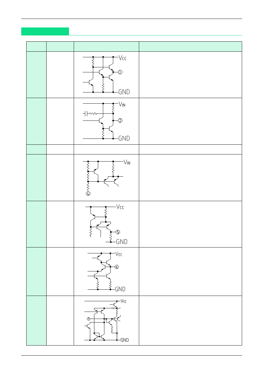
Control of Lithium Ion Battery Charging and Discharging MM1248
Pin no.
Pin name
Equivalent circuit
Function
1
DCHG
Pch-FET gate connector pin for discharge control
"L" output during discharge, "H" when discharge is
stopped
2
CHG
Pch-FET gate connector pin for charge control
Feedback loop for constant-voltage control formed
during charging; "H" output when charging is
stopped
When overvoltage or overheating is sensed (during
charging), the gate is turned off ("H" level).
4
CON
Input pin for charge control signal.
Input "L" to turn charging on, "H" to turn charging
off (when open, charging is off)
5
OV1
Overvoltage signal output pin. PNP output, with
internal pull-down resistance (50 k
typ.)
"L" output in normal operation, "H" output on
overvoltage
6
V
BAT
On discharge, 1/3 the battery module voltage is
output; when discharge stops, switches to high-
impedance output
7
CCC
Pin for connection to a capacitor to set the dead
time for overcharge detection
Normal operation : GND level; overcharge : approx.
5V
Dead time is approx 1S for an 0.068µF capacitance
3
V
IN
Power supply input pin for the charge control unit
Pin Description
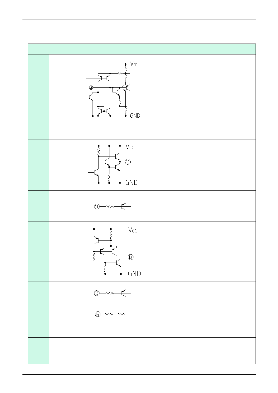
MITSUMI
Control of Lithium Ion Battery Charging and Discharging MM1248
Pin no.
Pin name
Equivalent circuit
Function
8
CDC
Pin for connection to a capacitor to set the dead
time for discharge on/off switching
During discharge : approx. 5V; when discharge
stops : GND level
Dead time is set when discharge is turned off and
discharge stopped
Dead time is approx. 1S for an 0.1µF capacitance
11
BATL
Pin for input of L cell+terminal voltage (in a battery
module with three cells in series, cells are defined,
starting from the high side, as the H cell, M cell
and L cell)
10
FET (G)
Pin for connection to P-ch FET gate for battery
module voltage level input
During discharge "L" is output; when discharge is
stopped switches to "H"
12
OV2
Pin for overvoltage signal output; NPN open
collector output
High-impedance output during normal operation;
switches to "L" on overcharge
The high-potential side of the pull-up resistance
should be 10 V max
14
FET (D)
Pin for connection to drain of P-ch FET for battery
module voltage level input
13
BATM
Pin for input of M cell+terminal voltage
16
V
CC
Power supply input pin for overcharge detection,
discharge control, battery module voltage
monitoring units
Voltage at same potential as B
ATH
should be input
15
B
ATH
Pin for input of H cell+terminal voltage
9
GND
GND pin for this IC