 | –≠–ª–µ–∫—Ç—Ä–æ–Ω–Ω—ã–π –∫–æ–º–ø–æ–Ω–µ–Ω—Ç: MM1270 | –°–∫–∞—á–∞—Ç—å:  PDF PDF  ZIP ZIP |

MITSUMI
Low-Output Voltage Low-Saturation Three-Pin Regulator MM1270
Low-Output Voltage Low-Saturation Three-Pin Regulator
Monolithic IC MM1270
Outline
MM1270 is targeted at the one-battery output voltage market, and is a compact low input/output voltage
differential stable power supply with ultra-low current consumption.
Features
1. Input voltage
10V max.
2. Input/output voltage differential
0.05V typ.
3. Input current for no load
15µA typ.
4. Output voltage
1.08V, 1.03V typ.
5. Current limiter circuit included
6. On/Off logic
CE pin
Output
LOW
OFF
HIGH
ON
Package
SOT-25A (MM1270CN, MM1270ZN)
Applications
1. Pagers
2. Headphone stereos
3. Portable equipment
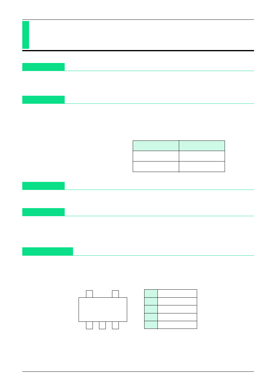
Pin Assignment
5
4
1
2
3
SOT-25A
1
V
OUT
2
GND
3
GND
4
CE
5
V
IN

MITSUMI
Low-Output Voltage Low-Saturation Three-Pin Regulator MM1270
Absolute Maximum Ratings
Item
Symbol
Rating
Units
Storage temperature
T
STG
-40~+125 ∞C
Operating temperature
T
OPR
-20~+75
∞C
Power supply voltage
V
CC
max.
-0.3~+10
V
CE pin voltage
V
CE
max.
-0.3~+10 V
Output current
Io max.
60
mA
Allowable loss
Pd
150
mW
Recommended Operating Conditions
Input voltage
V
IN
1.2~2.0
V
Output voltage
Io
0~10.0
mA
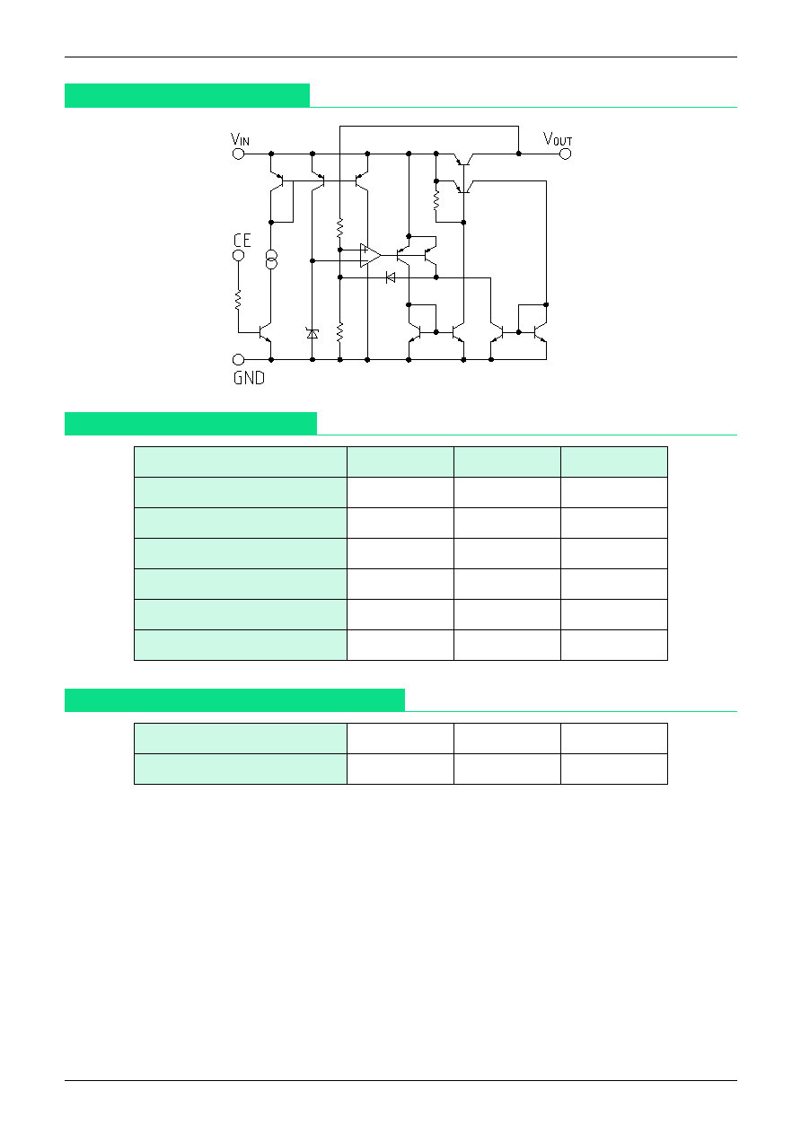
Equivalent Circuit Diagram

MITSUMI
Low-Output Voltage Low-Saturation Three-Pin Regulator MM1270
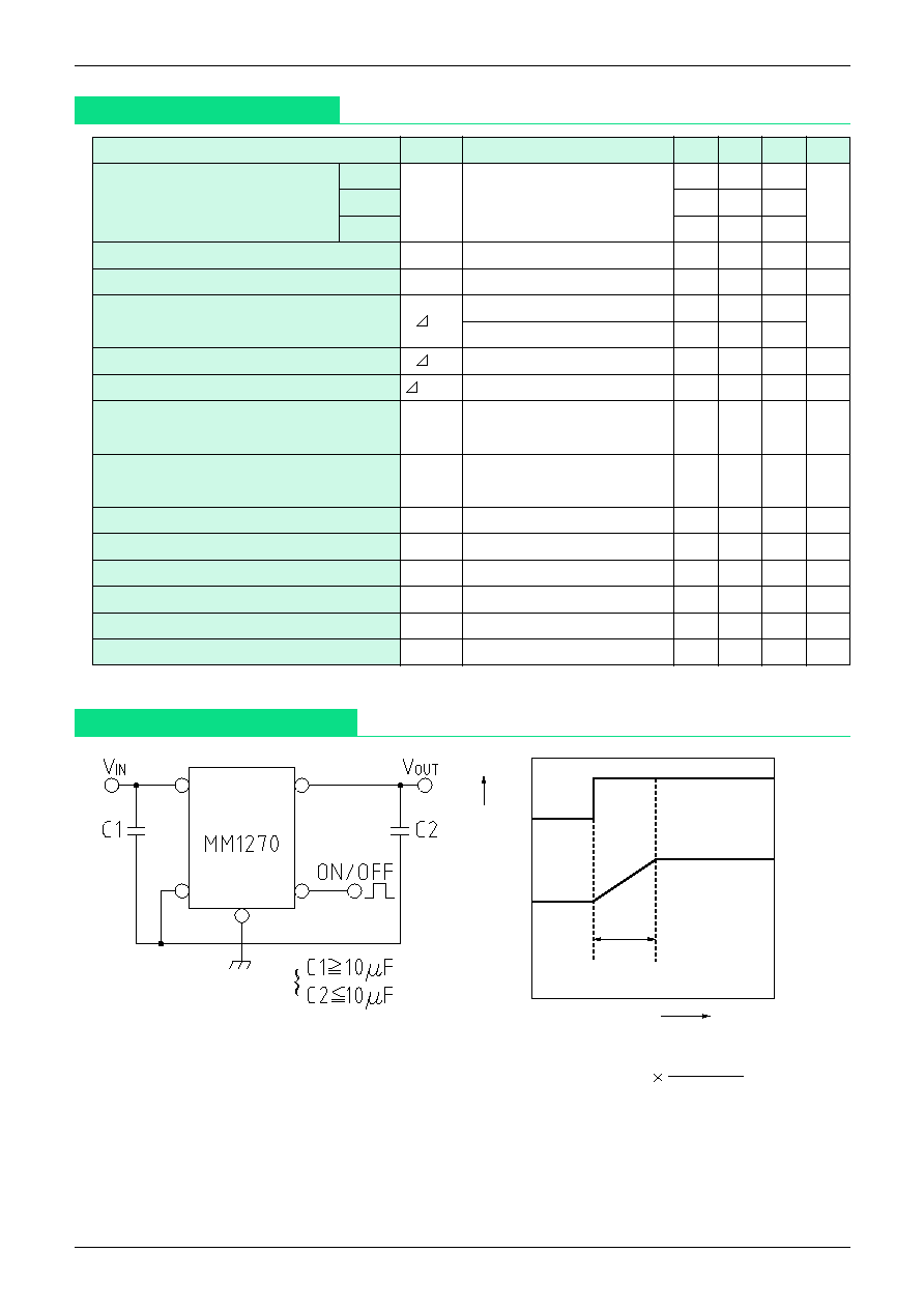
Equivalent Circuit Diagram
Tr
T
V
O
0
CE
L
H
V
*
Formula for output rise time.
Tr (µS) =C
OUT
(µF)
Vo (V)
I max.(A)
*
Note 1 : Locate the input/output capacitor as close as possible to the IC.
*
Note 2 : When not using output control, short the CE pin to the Vin pin.
Electrical Characteristics
(Ta=25∞C)
Item
Symbol
Measurement conditions
Min. Typ. Max. Units
Z rank
1.05
1.08
1.11
Output voltage
C rank
Vo
V
IN
=1.5V Io=1mA
1.00
1.03
1.06
V
D rank
1.200 1.235 1.270
No load input current
Iccq1
V
IN
=1.5V Io=0mA
15
35
µA
Minimum I/O voltage differential
Vd min.
V
IN
=1.0V Io=5mA
0.05
0.10
V
Input fluctuation ratio
V1
V
IN
=1.2V~1.25V Io=5mA
3
30
mV
V
IN
=1.25V~1.6V Io=5mA
10
20
Load fluctuation ratio
V2
V
IN
=1.5V Io=0~5mA
5
20
mV
Output voltage temperature coefficient
Vo/T
Tj=-20~+75∞C
+800
ppm/∞C
Ripple rejection rate
RR
V
IN
=1.5V f=120Hz
30
dB
V
RIPPLE
=0.1Vpp Io=5mA
Output noise voltage
VN
V
IN
=Vo+1V Io=100mA
150
µVrms
f=10~80kHz
Input current for OFF
Iccq2
V
IN
=1.5V, V
CE
=0.2V
1
µA
CE pin current for OFF
I
OFF
V
CE
=0.2V
-1
µA
CE pin current for ON
I
ON
V
CE
=1.5V
5
µA
CE pin HIGH level
H
0.8
10
V
CE pin LOW level
L
-0.3
0.2
V
Current limit
I max.
V
IN
=1.5V Ro=0
20
40
60
mA

MITSUMI
Low-Output Voltage Low-Saturation Three-Pin Regulator MM1270
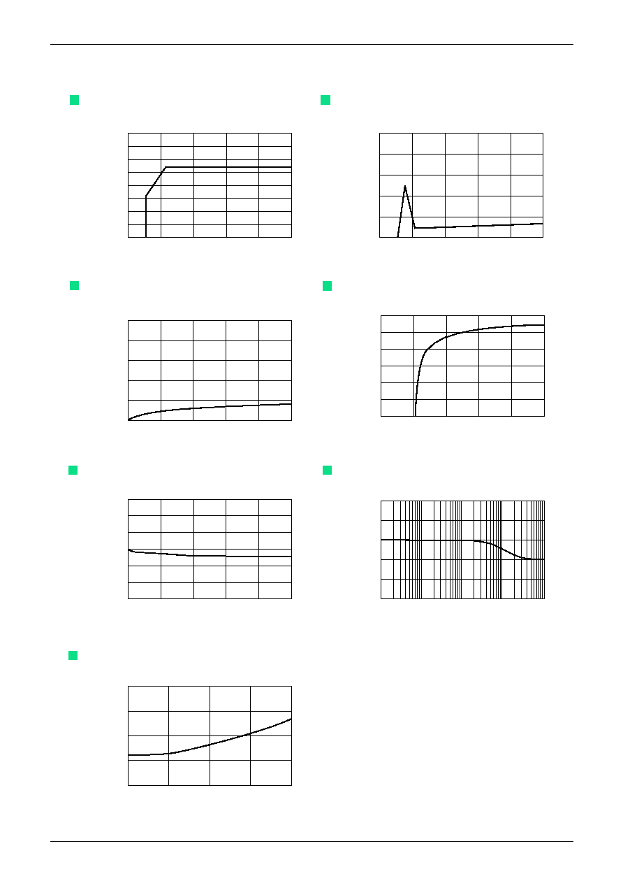
Output voltage characteristic (I
OUT
=0mA)
No-load input current
1.6
1.4
1.2
1
0.8
0.6
0.4
0.2
0
0
1
2
3
4
5
Output voltage (V)
Input voltage (V)
100
80
60
40
20
0
0
1
2
3
4
5
Input voltage (V)
No-load input current (
µ
A)
I/O voltage difference (V
IN
=1.0V)
0.25
0.2
0.15
0.1
0.05
0
0
2
4
6
8
10
Output current (mA)
I/O voltage difference
(
V
)
Input fluctuation
Load fluctuation
1.1
1.09
1.08
1.07
1.06
1.05
1.04
0
1
2
3
4
5
Input voltage (V)
Output voltage (V)
30
20
10
0
-10
-20
-30
0
2
4
6
8
10
Output current (mA)
Load fluctuation
(mV)
Ripple rejection rate (V
IN
=1.2V)
Output VS temperature
50
40
30
20
10
0
10
100
1000
10000
100000
Frequency (Hz)
Ripple rejection rate (dB)
1.2
1.15
1.1
1.05
1
-25
0
25
50
75
Temperature (
∞
C)
Output voltage (V)
