MITSUMI
High Precision Operational Amplifier MM1278
High Precision Operational Amplifier
Monolithic IC MM1278
Outline
This IC is a dual-type operational amplifier, with two built-in operational amplifiers, and achieves extremely
low offset voltage with a single power supply. The input offset voltage and the input offset voltage
temperature drift of this operation amplifier are one digit less than those of our conventional products. A
single power supply can be used, so there is no need to create a mid-point potential, and it can be operated
with the voltage from two batteries. Due to the single power supply, low current consumption, and low offset
voltage, two batteries can be used for operation, making it appropriate for equipment that amplifies the very
small signal of portable equipment.
Features
General
1. Power supply voltage
V
CC
=1.8V~6V
optimum for drive by batteries
2. Current consumption
0.1mA typ.
3. Power supply line elimination ratio
60dB typ.
Amplifier section
1. Input voltage range
-0.2V~+0.3V
2. Super low input offset voltage
±0.1mV typ.
3. Input offset voltage
±1µV/∞C typ.
4. Input offset current
1nA typ.
5. Input bias current
50nA typ.
6. Voltage gain
100dB typ.
Package
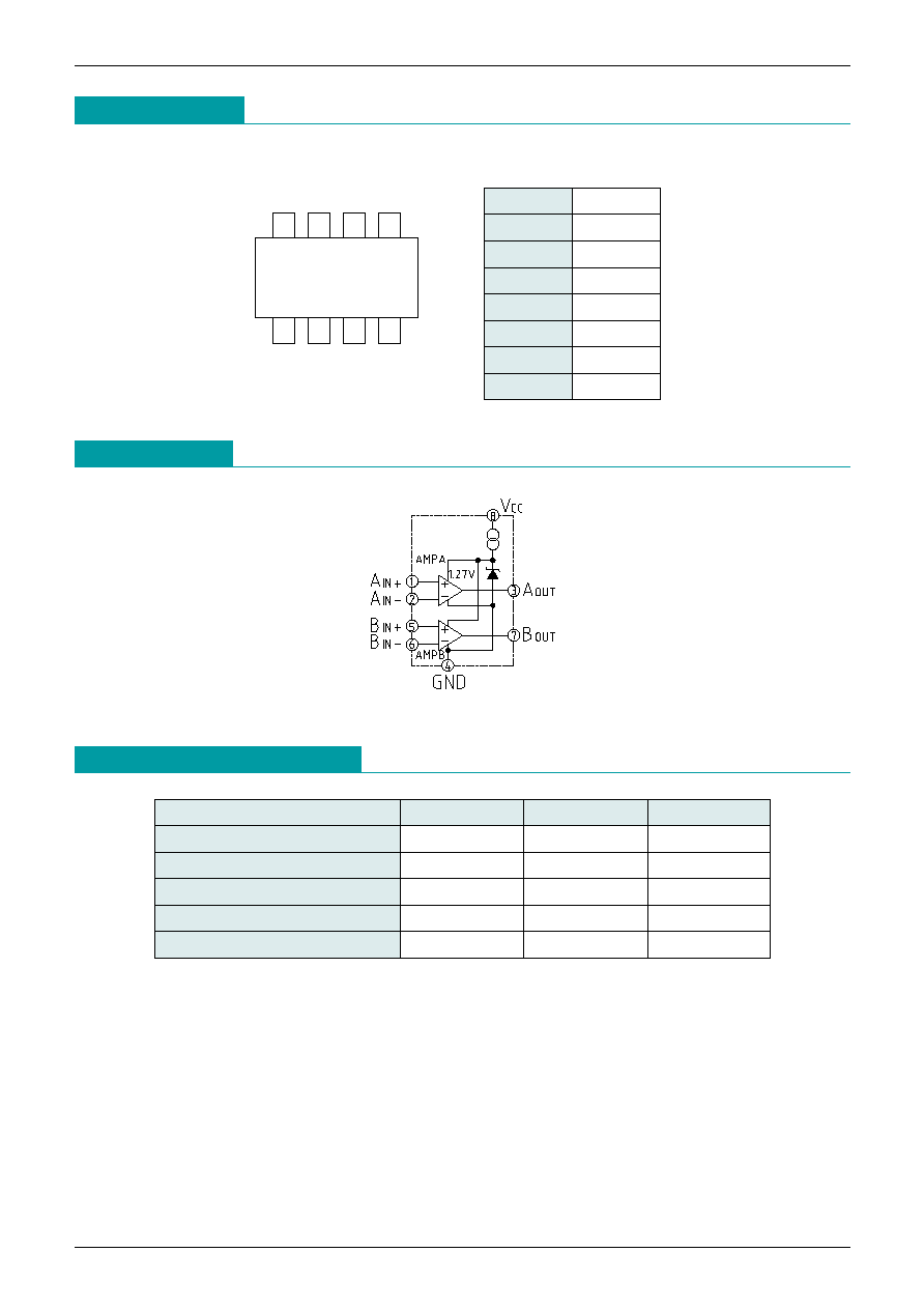
SOP-8D (MM1278XA)
DIP-8A (MM1278XD)
Applications
1. Amplification and detection of normal very small voltage on portable equipment.
2. Amplification of very small voltage for sensors (thermocouples, strain gauges, magnetic sensors)
3. Detedtion of very small current

MITSUMI
High Precision Operational Amplifier MM1278
Item
Symbol
Measurement Conditions
Min. Typ. Max. Units
Current consumption
I
CC
0.1
0.15
mA
Power supply line elimination ratio
P
SRR
f=100Hz
50
60
dB
Power supply voltage range
V
CC
1.8
3.0
6.0
V
Input voltage range
V
I
-0.2
0.3
V
Input offset voltage
V
IOA
±0.1 ±0.35
mV
Input offset voltage
temperature drift
V
IOA
Ta=-20~+70∞C
±1
±3
µV/∞C
Input offset current
I
IOA
1
10
nA
Input bias current
I
BA
50
150
nA
Voltage gain
G
V
R
L
=100k
80
100
dB
Output current
I
OA
V
IN
=10mV, V
O
=0.5V
0.5
mA
Output voltage
V
OA
V
IN
=-5~-25mV
V
CC
R
L
=10k
0.01
-1.0
V
Amplifier
section
Electrical Characteristics
(Unless otherwise specified Ta=25∞C, V
CC
=3V, V
IN
=0V)
Note : Use a gain range of 20dB ~ 50dB in the amplifier section (40dB recommended).
Also, insert the capacitor between output and GND, instead of parallel to the gain setting feedback
resistor, in order to eliminate noise from the input.
Please note that use of the equipment under different conditions will cause vibration.


