MITSUMI
Protection of Lithium Ion Battery (three cells in series) MM1309
Protection of Lithium Ion Batteries (three cells in series)
Monolithic IC MM1309
Outline
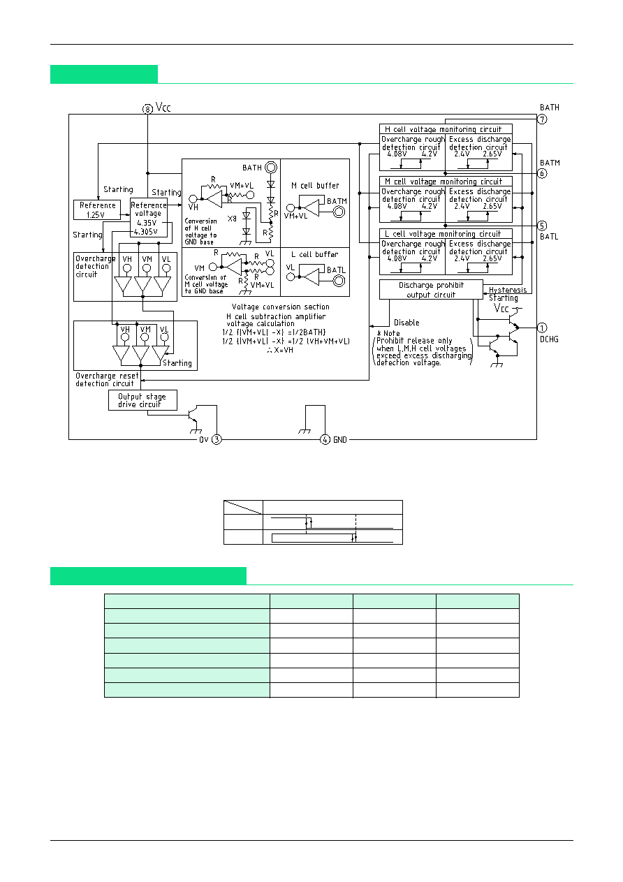
This is a 3-cell series protection IC is for protecting a lithium ion battery from overcharging and excess
discharging. If abnormalities occur during charging and excess voltage is applied, it has a function that turns
off the external FET switch (overcharging detection). It also has a function that turns off the external FET
switch when the voltage for each battery falls below a set voltage, to prevent excess discharge when
discharging the battery (discharging detection). At that time, the IC is switched to low current consumption
mode.
These functions comprise a protection circuit, with few external parts, for lithium ion batteries.
Features
1. Current consumption (for V
CC
pin)
V
CELL
=4.4V
700µA typ.
2. Current consumption (for V
CC
pin)
V
CELL
=4.2V
300µA typ.
3. Current consumption (for V
CC
pin)
V
CELL
=3.8V
25µA typ.
4. Current consumption (for V
CC
pin)
V
CELL
=2.2V
0.1µA max.
5. Current consumption (for BATH pin)
V
CELL
=4.4V
12µA typ.
6. Current consumption (for BATH pin)
V
CELL
=3.8V
8µA typ.
7. Current consumption (for BATH pin)
V
CELL
=2.2V
1µA typ.
8. Charge prohibit voltage (Ta=-20∞C~+70∞C)
B : 4.35V±50mV
C : 4.25V±50mV
9. Charge prohibit release voltage
V
CELLU
-45mV
10.Charge prohibit detection function operation voltage
B : 4.20V typ.
C : 4.10V typ.
11.Excess discharge detection voltage
2.40V±0.09V, 2.35V±0.09V
12.Discharge resumption voltage
B : 2.65V±0.16V
C : 2.60V±0.16V
13.Excess discharge detection hysteresis voltage
250±75mV
Package
SOP-8C (MM1309 F)
*
The box represents the rank resulting from the combination of protection functions.
Applications
1. Notebook PCs
2. Portable terminals
3. Others
MITSUMI
Protection of Lithium Ion Battery (three cells in series) MM1309
Pin Assignment
1
4
3
2
8
5
6
7
SOP-8C
Pin Description
1
D
CHG
2
N. C
3
OV
4
GND
5
B
ATL
6
B
ATM
7
B
ATM
8
V
CC
No.
Pin
Output
Function
1
D
CHG
Output
2
N. C
3
OV
Output
4
GND
5
B
ATL
Input
6
B
ATM
Input
7
B
ATM
Input
8
V
CC
FET drive pin for excess discharge control
FET drive pin for overcharge control
Negative connection pin for the low side battery. Also, IC GND pin.
(IC reference power supply pin)
Positive connection pin for the low side battery, and negative connection pin for the
middle side battery.
Positive connection pin for the middle side battery, and negative connection pin for
the high side battery.
Positive connection pin for the high side battery.
IC positive power supply input pin.
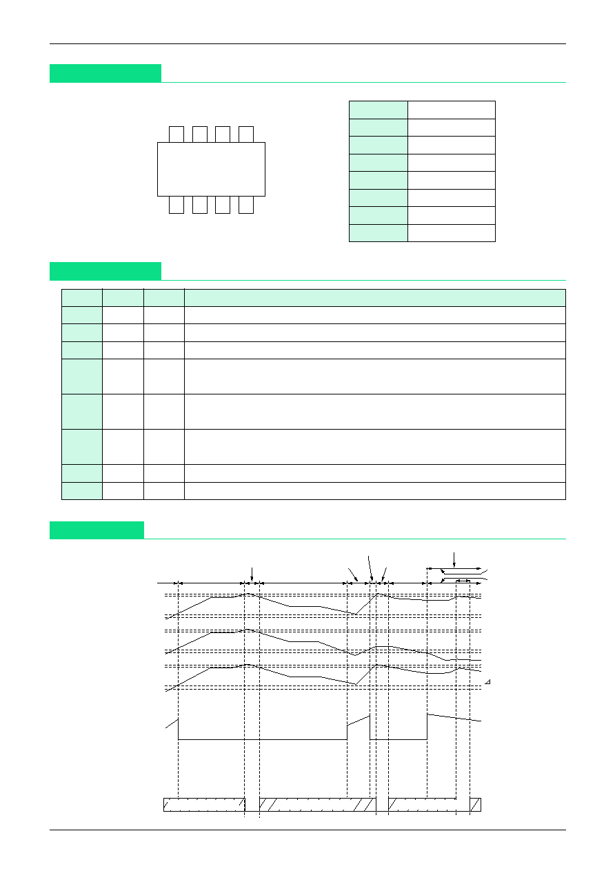
Timing Chart
High Impedance
High Impedance
High Impedance
V
CELL
U
V
CELL
O
V
CELL
D
V
CELL
S
V
CELL
U
V
CELL
O
V
CELL
D
V
CELL
S
V
CELL
O
V
CELL
D
V
CELL
S
B
ATM
B
ATH
B
ATL
V
ALM
V
ALM
V
ALM
D
CHG
OV
H
L
L
Excess discharge
Normal
Overcharge
Normal
Excess discharge
Overcharge
Normal
Overcharge
Excess discharge
Normal
Unbalanced (large voltage differences)
V
CELL
U
MITSUMI
Protection of Lithium Ion Battery (three cells in series) MM1309
Electrical Characteristics
(Unless otherwise specified Ta=25∞C, V
IN
=15V, V
CELL
=V
BAT
H=V
BAT
M=V
BAT
L)
Item
Symbol
Measurement Conditions
Min
Typ. Max. Units
Current consumption (V
CC
pin) 1
I
CC
1
V
CELL
=4.4V
0.7
1.1
mA
Current consumption (V
CC
pin) 2
I
CC
2
V
CELL
=4.2V
300
450
µA
Current consumption (V
CC
pin) 3
I
CC
3
V
CELL
=3.8V
25.0
40.0
µA
Current consumption (V
CC
pin) 4
I
CC
4
V
CELL
=2.3V
0.1
µA
Current consumption (BATH pin) 1
I
BATH
1
V
CELL
=4.4V
12.0
20.0
µA
Current consumption (BATH pin) 2
I
BATH
2
V
CELL
=3.8V
8.0
12.0
µA
Current consumption (BATH pin) 3
I
BATH
3
V
CELL
=2.3V
1.0
2.0
µA
Charge prohibit voltage
MM1309BF
V
CELL
U
Ta=-20~70∞C
4.30
4.35
4.40
V
MM1309CF
V
CELL
=4.0V 4.5V
4.20
4.25
4.30
Charge prohibit release voltage
V
CELL
O
V
CELL
=4.5V 4.0V
V
CELL
U V
CELL
U V
CELL
U
V
-60mV -45mV -30mV
Charge prohibit detection
MM1309BF
V
ALM
V
CELL
=3.8V 4.4V
4.05
4.20
4.25
V
function operation voltage MM1309CF
3.95
4.10
4.25
Charge prohibition sensing operation
voltage Hysteresis voltage
V
ALM
V
CELL
=4.4V 3.8V
50
90
130
mV
Excess discharging
MM1309BF
V
CELL
S
V
CELL
=3.0V 2.0V
2.31
2.40
2.49
V
detection voltage
MM1309CF
2.26
2.35
2.44
Discharge resumption
MM1309BF
V
CELL
D
V
CELL
=2.0V 3.0V
2.49
2.65
2.81
V
voltage
MM1309CF
2.44
2.60
2.76
Excess discharge detection
V
CS
D
V
CELL
D-V
CELL
S
175
250
325
mV
hysteresis voltage
BATL pin input voltage 1
I
BAT
L
V
CELL
=3.8V
±300
nA
BATL pin input voltage 2
I
BAT
LA
V
CELL
=4.4V
0.7
1.0
1.3
uA
BATM pin input voltage 1
I
BAT
M
V
CELL
=3.8V
±300
nA
BATM pin input voltage 2
I
BAT
MA
V
CELL
=4.4V
0.7
1.0
1.3
uA
DCHG pin source voltage
I
SO
D
CH
V
CELL
< V
CELLS
20
uA
DCHG sink voltage
I
SI
D
CH
V
CELL
> V
CELLS
20
uA
DCHG output voltage L
V
TH
D
C
L
B
AT
H-D
CHG
IS=20uA
1.0
V
DCHG output voltage M
V
TH
D
C
H
D
CHG
-GND IS=-20uA
0.8
V
OV pin sink current
I
SI
O
V
VO
V
=0.4, Ta=-20~70∞C
200
uA
Application