
MITSUMI
I
2
C BUS Control 5-Input 2-Output AV Switch MM1313
I
2
C BUS Control 5-Input 2-Output AV Switch
Monolithic IC MM1313
Outline
This IC is a 5-input 2-output AV switch with I
2
C control, developed for use in televisions. Two outputs enable
it to support two screens or "picture-in-picture".
Features
1. Serial control by I
2
C bus.
2. 5-inputs, 2-outputs.
3. Video and audio system switches can be controlled independently.
4. 6dB amplifier built in to video system.
5. Built-in Y/C MIX circuit.
6. Slave address can be changed : 90H or 92H.
7. Audio muting possible by external pin.
8. Maintains high impedance even when I
2
C BUS line (SDA, SCL) power supply is off.
9. Built-in 3 value discrimination function.
10.On-chip power ON reset function.
11.Two types of audio input impedance : 60k
and 30k
.
MM1313AD : 60k
MM1313BD : 30k
12.Supports 2-screen or P-IN-P TV.
Package
SDIP-42A (MM1313AD, MM1313BD)
Applications
1. Televisions
2. Other video equipment
MITSUMI
I
2
C BUS Control 5-Input 2-Output AV Switch MM1313
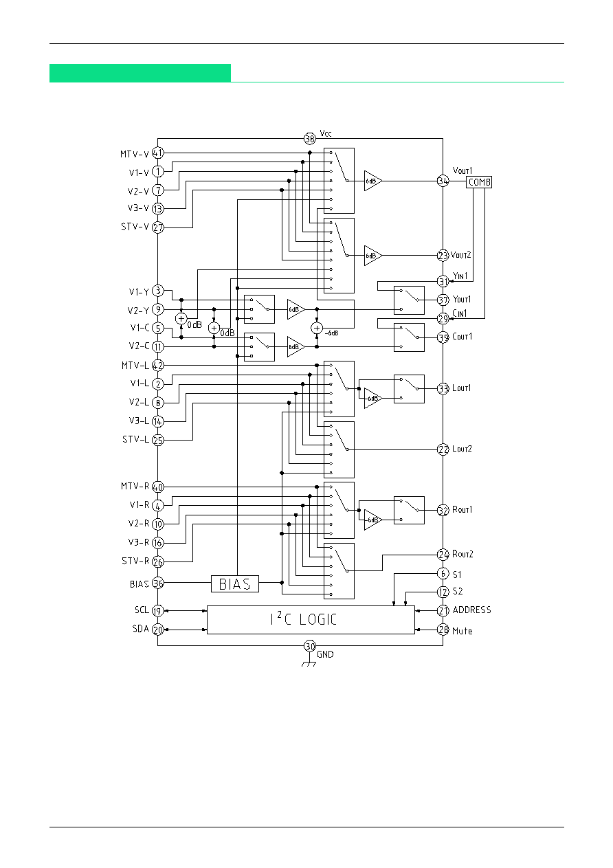
Equivalent Block Diagram

MITSUMI
I
2
C BUS Control 5-Input 2-Output AV Switch MM1313
Pin Function
Pin No.
Name
Internal equivalent circuit diagram Pin No.
Name
Internal equivalent circuit diagram
41
MTV-V
1
V1-V
7
V2-V
13
V3-V
27
STV-V
3
V1-Y
9
V2-Y
31
Y
IN
1
5
V1-C
11
V2-C
29
C
IN
1
42
MTV-L
2
V1-L
8
V2-L
14
V3-L
25
STV-L
40
MTV-R
4
V1-R
10
V2-R
16
V3-R
26
STV-R
34
V
OUT
1
23
V
OUT
2
37
Y
OUT
1
39
C
OUT
1
33
L
OUT
1
22
L
OUT
2
32
R
OUT
1
24
R
OUT
2
36
BIAS
19
SCL
20
SDA
6
S1
12
S2
21
ADR
28
Mute

MITSUMI
I
2
C BUS Control 5-Input 2-Output AV Switch MM1313
Absolute Maximum Ratings
(Ta=25
�C
)
Item
Symbol
Ratings
Units
Storage temperature
T
STG
-40~+125
�
C
Operating temperature
T
OPR
-20~+75
�
C
Power supply voltage
V
CC
12
V
Allowable power dissipation
Pd
850
mW
Electrical Characteristics
(Ta=25�C, V
CC
=9V)
Item
Symbol
Measure Conditions (unless otherwise indicated,
Min. Typ. Max. Units
ment pin
Measurement Circuit Figure 1)
Operating power supply voltage
V
CC
8
9
10
V
Current consumption
I
CC
38
V
CC
=9V, no signal, no load
40
52
mA
V
OUT
1 output
Voltage gain
G
V
1
TP1
Sine wave 1.0V
P-P
, 100kHz
5.5
6.0
6.5
dB
Frequency characteristics
F
V
1
TP1
Sine wave 1.0V
P-P
, 10MHz/100kHz
-1.0
0
1.0
dB
Vn-V : Staircase 1V
P-P
APL=10~90%
Differential gain
DG
V
1
TP1
Vn-Y : Staircase (luminance signal) 1V
P-P
-3
0
3
%
Vn-C : Chroma signal 0.3V
P-P
APL=10~90%
Vn-V : Staircase 1V
P-P
APL=10~90%
Differential phase
DP
V
1
TP1
Vn-Y : Staircase (luminance signal) 1V
P-P
-3
0
3
deg
Vn-C : Chroma signal 0.3V
P-P
APL=10~90%
Sine wave 100kHz
Input dynamic range
D
V
1
SG1~3
Maximum input for total higher
1.6
1.9
V
P-P
harmonic distortion factor < 1.0%
V
OUT
2 output
Voltage gain
G
V
2
TP6
Sine wave 1.0V
P-P
, 100kHz
5.5
6.0
6.5
dB
Frequency characteristics
F
V
2
TP6
Sine wave 1.0V
P-P
-1.0
0
1.0
dB
10MHz/100kHz
Vn-V : Staircase 1V
P-P
APL=10~90%
Differential gain
DG
V
2
TP6
Vn-Y : Staircase (luminance signal) 1V
P-P
-3
0
3
%
Vn-C : Chroma signal 0.3V
P-P
APL=10~90%
Vn-V : Staircase 1V
P-P
APL=10~90%
Differential phase
DP
V
2
TP6
Vn-Y : Staircase (luminance signal) 1V
P-P
-3
0
3
deg
Vn-C : Chroma signal 0.3V
P-P
APL=10~90%
Sine wave 100kHz
Input dynamic range
D
V
2
SG1~3
Maximum input for total higher
1.6
1.9
V
P-P
harmonic distortion factor < 1.0%
Y
OUT
1 output
Voltage gain
G
Y
1
TP2
Vn-Y : Sine wave 1.0V
P-P
, 100kHz
5.5
6.0
6.5
dB
G
Y
2
TP2
Y
IN
1 : Sine wave 2.0V
P-P
, 100kHz
-0.5
0
0.5
F
Y
1
TP2
Vn-Y : Sine wave 1.0V
P-P
-1.0
0
1.0
Frequency characteristics
10MHz/100kHz
dB
F
Y
2
TP2
Y
IN
1 : Staircase 2.0V
P-P
-1.0
0
1.0
10MHz/100kHz
Vn-Y : Staircase 1V
P-P
Differential gain
DG
Y
TP2
APL=10~90%
-3
0
3
%
Y
IN
1: Staircase 2V
P-P
APL=10~90%
Vn-Y : Staircase 1V
P-P
Differential phase
DP
Y
TP2
APL=10~90%
-3
0
3
deg
Y
IN
1 : Staircase 2V
P-P
APL=10~90%

MITSUMI
I
2
C BUS Control 5-Input 2-Output AV Switch MM1313
Item
Symbol
Measure Conditions (unless otherwise indicated,
Min. Typ. Max. Units
ment pin
Measurement Circuit Figure 1)
Vn-Y : Sine wave 100kHz
D
Y
1
SG2
Maximum input for total higher
1.6
1.9
Input dynamic range
harmonic distortion factor < 1.0%
V
IN
1 : Sine wave 100kHz
V
P-P
D
Y
2
SG4
Maximum input for total higher
3.2
3.8
harmonic distortion factor < 1.0%
Output impedance
Z
OYC
1
50
C
OUT
1 output
Voltage gain
G
C
1
TP3
Vn-C : Sine wave 1.0V
P-P
, 100kHz
5.5
6.0
6.5
dB
G
C
2
TP3
C
IN
1 : Sine wave 2.0V
P-P
, 100kHz
-0.5
0
0.5
F
C
1
TP3
Vn-C : Sine wave 1.0V
P-P
-1.0
0
1.0
Frequency characteristics
10MHz/100kHz
dB
F
C
2
TP3
C
IN
1 : Sine wave 2.0V
P-P
-1.0
0
1.0
10MHz/100kHz
Differential gain
DG
C
TP3
C
IN
1 : Staircase 2V
P-P
-3
0
3
%
APL=10~90%
Differential phase
DP
C
TP3
C
IN
1 : Staircase 2V
P-P
-3
0
3
deg
APL=10~90%
Vn-C : Sine wave 100kHz
D
C
1
SG3
Maximum input for total higher
2.75
3.25
Input dynamic range
harmonic distortion factor < 1.0%
V
P-P
C
IN
1: Sine wave 100kHz
D
C
2
SG5
Maximum input for total higher
5.5
6.5
harmonic distortion factor < 1.0%
Input impedance
Z
IC
Vn-C, C
IN
1
10
15
20
k
Output impedance
Z
OC
1
50
L
OUT
1 output
Voltage gain
G
L
11
TP4
b7=0, Sine wave 2.5V
P-P
, 1kHz
-6.5
-6.0
-5.5
dB
G
L
12
TP4
b7=1, Sine wave 2.5V
P-P
, 1kHz
-0.5
0.0
0.5
Frequency characteristics
F
L
1
TP4
Sine wave 2.5V
P-P
, 1MHz/1kHz
-3.0
0
1.0
dB
Total higher harmonic distortion
THD
L
1
TP4
Sine wave 2.5V
P-P
, 1kHz
0.03
0.1
%
Sine wave 1kHz
Input dynamic range
D
L
1
SG6
Maximum input for total higher
2.6
2.8
Vrms
harmonic distortion factor < 0.5%
Output offset voltage
V
OFFL
1
33
L
OUT
1 pin DC difference during
0
�15
mV
SW switching
Input impedance
Z
IL
1
42
60
78
k
Output impedance
Z
OL
1
120
L
OUT
2 output
Voltage gain
G
L
2
TP7
Sine wave 2.5V
P-P
, 1kHz
-0.5
0.0
0.5
dB
Frequency characteristics
F
L
2
TP7
Sine wave 2.5V
P-P
, 1MHz/1kHz
-3.0
0
1.0
dB
Total higher harmonic distortion
THD
L
2
TP7
Sine wave 2.5V
P-P
, 1kHz
0.03
0.1
%
Sine wave 1kHz
Input dynamic range
D
L
2
SG6
Maximum input for total higher
2.6
2.8
Vrms
harmonic distortion factor < 0.5%
Output offset voltage
V
OFFL
2
22
L
OUT
2 pin DC difference during
0
�15
mV
SW switching
Output impedance
Z
OL
2
120
R
OUT
1 output
Voltage gain
G
R
11
TP5
b7=0, Sine wave 2.5V
P-P
, 1kHz
-6.5
-6.0
-5.5
dB
G
R
12
TP5
b7=1, Sine wave 2.5V
P-P
, 1kHz
-0.5
0.0
0.5
Frequency characteristics
F
R
1
TP5
Sine wave 2.5V
P-P
, 1MHz/1kHz
-3.0
0
1.0
dB
Total higher harmonic distortion
THD
R
1
TP5
Sine wave 2.5V
P-P
, 1kHz
0.03
0.1
%
Sine wave 1kHz
Input dynamic range
D
R
1
SG7
Maximum input for total higher
2.6
2.8
Vrms
harmonic distortion factor < 0.5%
Output offset voltage
V
OFFR
1
32
R
OUT
1 pin DC difference during
0
�15
mV
SW switching
Input impedance
Z
IR
1
42
60
78
k
Output impedance
Z
OR
1
120
MITSUMI
I
2
C BUS Control 5-Input 2-Output AV Switch MM1313
Item
Symbol Measure Conditions (unless otherwise indicated, Min. Typ. Max. Units
ment pin
Measurement Circuit Figure 1)
R
OUT
2 output
Voltage gain
G
R
2
TP8
Sine wave 2.5V
P-P
, 1kHz
-0.5
0.0
0.5
dB
Frequency characteristics
F
R
2
TP8
Sine wave 2.5V
P-P
, 1MHz/1kHz
-3.0
0
1.0
dB
Total higher harmonic distortion
THD
R
2
TP8
Sine wave 2.5V
P-P
, 1kHz
0.03
0.1
%
Sine wave 1kHz
Input dynamic range
D
R
2
SG7
Maximum input for total higher
2.6
2.8
Vrms
harmonic distortion factor < 0.5%
Output offset voltage
V
OFFR
2
24
R
OUT
2 pin DC difference during
0
�15
mV
switching
Output impedance
Z
OR
2
120
Crosswalk
V
OUT
1
C
TV
1
TP1
Measurement Circuit Figure 2
-60
-53
dB
V
OUT
2
C
TV
2
TP2
for SG1 input : 4.43MHz, 1V
P-P
-60
-53
dB
Y
OUT
1
C
TY
1
TP3
for SG2 input : 4.43MHz, 0.5V
P-P
-60
-53
dB
C
OUT
1
C
TC
1
TP6
-60
-53
dB
L
OUT
1
C
TL
1
TP4
-90
-80
dB
L
OUT
2
C
TL
2
TP5
Measurement Circuit Figure 2
-90
-80
dB
R
OUT
1
C
TR
1
TP7
1kHz, 2.5V
P-P
-90
-80
dB
R
OUT
2
C
TR
2
TP8
-90
-80
dB
Video I/O Pin Voltage
Input pin voltage
V
VIP
No signal, no load
4.6
4.9
5.2
V
V
VOP
V
OUT
1 pin, V
OUT
2 pin
4.1
4.4
4.7
V
Output pin voltage
No signal, no load
V
SOP
Y
OUT
1 pin, C
OUT
1 pin
3.3
3.6
3.9
V
No signal, no load
Audio I/O Pin Voltage
Input pin voltage
V
AIP
No signal, no load
4.0
4.3
4.6
V
Output pin voltage
V
AOP
No signal, no load
3.9
4.2
4.5
V
Logic section (Refer to figure below)
Input voltage L
V
IL
I
2
C logic low level discrimination value
0.0
1.5
V
Input voltage H
V
IH
I
2
Clogic high level discrimination value
3.0
5.0
V
Low level output voltage (SDA)
V
OL
SDA for 3mA inflow
0.0
0.4
V
High level input current
I
IH
when SDA, SCL=4.5V impressed
-10
+10
�A
Low level input current
I
IL
when SDA, SCL=0.4V impressed
-10
+10
�A
Clock frequency
f
SCL
100
kHz
Data transmission waiting time
t
BUF
4.7
�S
SCL start hold time
t
HD;STA
4.0
�S
SCL low level hold time
t
LOW
4.7
�S
SCL high level hold time
t
HIGH
4.0
�S
SCL start set-up time
t
SU;STA
4.7
�S
SDA data hold time
t
HD;DAT
200
nS
SDA data set-up time
t
SD;DAT
250
nS
SCL rise time
t
R
1000
nS
SCL fall time
t
F
300
nS
SCL stop set-up time
t
SU;STO
4.0
�S
SDA
SCL
t
BUF
P
P
S t
HD:STA
t
HD:DAT
t
HIGH
t
SU:DAT
t
SU:STA
t
SU:STD
t
LOW
Sr
t
R
t
F
I
2
C BUS BUS Control Signal
MITSUMI
I
2
C BUS Control 5-Input 2-Output AV Switch MM1313
Measurement Circuit
Measurement Circuit 1
MITSUMI
I
2
C BUS Control 5-Input 2-Output AV Switch MM1313
Measurement Circuit 2 (Crosstalk measurement)
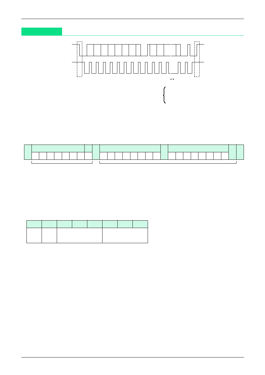
The I
2
C BUS is a BUS system developed by Philips for internal use in equipment. Data transmission is carried
out by the two SDA and SCL lines, in byte units, with the MSB first from start condition.
[Control Register]
The control register contains data sent from the master in order to determine the status of each switch.
The data format is set as shown in the figure above. The first 7 bits in the address byte are allocated to the
slave address, and the remaining 1 bit is allocated to the read/write bit. The read/write bit is set at 0 when
using as a control register.
The MM1313 slave address can be selected as 90H/92H depending on the status of the ADR pin. When ADR
pin is low it is 90H.
The relationship between the control register bits and switch control is as shown below.
The control register bits are reset to 0 when power is applied.
MM1313 control is carried out by the 3-byte structure of the 1 address byte and 2 control data bytes. The first
byte in the control data is control data for output 1, and the remaining 1 byte is control data for output 2.
All of the remaining data (fourth byte and after) are ignored.
Refer to the separate tables for details on switch control.
MITSUMI
I
2
C BUS Control 5-Input 2-Output AV Switch MM1313
I
2
C BUS
SDA
SCL
S
1
2
3
4
5
6
7
8
A
1
2
3
8
A
P
S:Start Condition
P:Stop Condition
A:Acknowledge
Address byte
Control data
S
Slave address
R/W
1
0
0
1
0
0 0/1 0
A
Control register 1
b7 b6 b5 b4 b3 b2 b1 b0
A
Control register 2
b7 b6 b5 b4 b3 b2 b1 b0
A
P
b7
b6
b5
b4
b3
b2
b1
b0
Audio S/Comp
Video-Select
Audio-Select
Gain
Select
MITSUMI
I
2
C BUS Control 5-Input 2-Output AV Switch MM1313
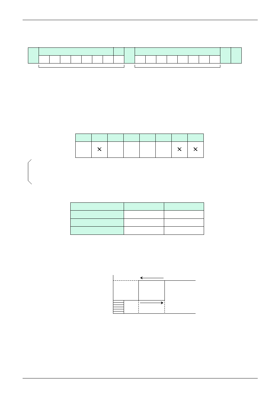
[Status Register]
The status register contains data for sending device status to the master.
The data format is set as shown in the figure above. The first 7 bits in the address byte are allocated to the
slave address, and the remaining 1 bit is allocated to the read/write bit. The read/write bit is set at 1 when
using as a status register.
The MM1313 slave address can be selected as 91H/93H depending on the status of the ADR pin. When the
ADR pin is low it is 91H. However, the confirmation response after completion of the status register should be
non-acknowledge.
The status register output data as shown below.
P-ON RESET : Returns 1 for power on reset. However once data read begins, 0 is returned next.
S1/S2 OPEN : Returns 0 when the S1/S2 pin is not open, and returns 1 when the S1/S2 pin is open
S1/S2 SEL : Returns 0 when the S1/S2 pin is not grounded, and returns 1 when the S1/S2 pin is grounded.
S1/S2 OPEN, SEL have 3-value discrimination, and the combinations are as shown below.
[Power On Reset]
Power on reset is built in to reset each control register to 0 when power is turned on.
Power on reset threshold has hysteresis as shown in the figure below. The IC power on reset status can be
discriminated by reading the status register P-ON RESET.
S
Slave address
R/W
A
Status register
NA
P
1
0
0
1
0
0
0/1
1
b7
b6
b5
b4
b3
b2
b1
b0
Address byte
Status data
b7
b6
b5
b4
b3
b2
b1
b0
P-ON
S1
S1
S2
S2
RESET
OPEN
SEL
OPEN
SEL
S1/S2 pin DC voltage
S1/S2 OPEN
S1/S2 SEL
0.8V or less
0
1
1.3V or more, 3.5V or less
0
0
4.5V or more
1
0
Reset released
Reset status
Undefined
0.6V
4.3V
5.4V
V
CC
MITSUMI
I
2
C BUS Control 5-Input 2-Output AV Switch MM1313
Switch Control Table
b6
b5
b4
b3
V
OUT
1
Y
OUT
1
C
OUT
1
0
0
0
0
Mute
Mute
Mute
0
0
0
1
MTV-V
Y
IN
1
C
IN
1
0
0
1
0
V1-V
Y
IN
1
C
IN
1
0
0
1
1
V2-V
Y
IN
1
C
IN
1
0
1
0
0
V3-V
Y
IN
1
C
IN
1
0
1
0
1
STV-V
Y
IN
1
C
IN
1
0
1
1
0
Mute
Mute
Mute
1
1
1
0
0
0
Mute
Mute
Mute
1
0
0
1
MTV-V
Y
IN
1
C
IN
1
1
0
1
0
V1-Y+C
V1-Y
V1-C
1
0
1
1
V2-Y+C
V2-Y
V2-C
1
1
0
0
V3-V
Y
IN
1
C
IN
1
1
1
0
1
STV-V
Y
IN
1
C
IN
1
1
1
1
0
Mute
Mute
Mute
1
1
Mute pin
b2
b1
b0
L
OUT
1
R
OUT
1
0
0
0
Mute
Mute
0
0
1
MTV-L
MTV-R
0
1
0
V1-L
V1-R
1.5V or less
0
1
1
V2-L
V2-R
(OPEN)
1
0
0
V3-L
V3-R
1
0
1
STV-L
STV-R
1
1
0
Mute
Mute
1
1
3.0V or more
-
-
-
Mute
Mute
Mute pin
b2
b1
b0
L
OUT
2
R
OUT
2
0
0
0
Mute
Mute
0
0
1
MTV-L
MTV-R
0
1
0
V1-L
V1-R
1.5V or less
0
1
1
V2-L
V2-R
(OPEN)
1
0
0
V3-L
V3-R
1
0
1
STV-L
STV-R
1
1
0
Mute
Mute
1
1
3.0V or more
-
-
-
Mute
Mute
b6
b5
b4
b3
V
OUT
2
0
0
0
0
Mute
0
0
0
1
MTV-V
0
0
1
0
V1-V
0
0
1
1
V2-V
0
1
0
0
V3-V
0
1
0
1
STV-V
0
1
1
0
Mute
1
1
1
0
0
0
Mute
1
0
0
1
MTV-V
1
0
1
0
V1-Y+C
1
0
1
1
V2-Y+C
1
1
0
0
V3-V
1
1
0
1
STV-V
1
1
1
0
Mute
1
1
b7
Output gain
0
-6dB output
1
0dB output
1. Video Output 1
3. Audio Output 1
5. Audio Output 2
4. Audio Output 1 Gain
Switching
2. Video Output 2
MITSUMI
I
2
C BUS Control 5-Input 2-Output AV Switch MM1313
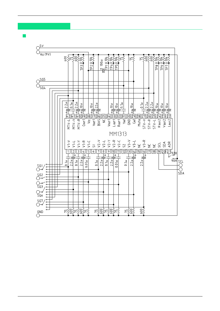
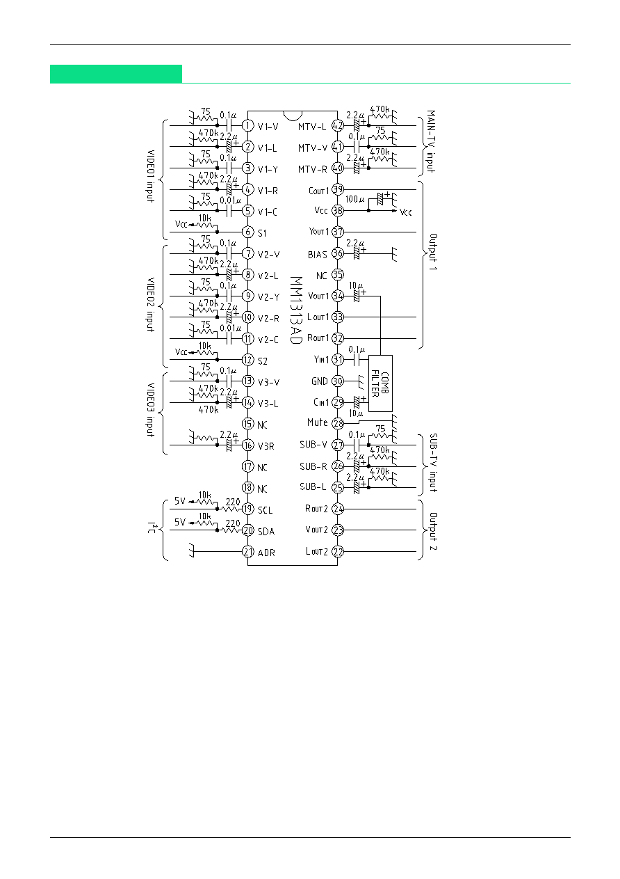
Application Circuit
Notes
1. V
OUT
is set at 4.4V and C
IN
at 4.9V
Please note that capacitance polarity may vary depending on comb filter bias.
2. Each audio output can be muted by making pin 19 high. Mute is off when it is open or low.