MITSUMI
LCD Interface MM1323
LCD Interface
Monolithic IC MM1323
Outline
This IC was developed for interface with digital video equipment having an LCD monitor.
It can be used as interface for CPU, DSP and LCD drivers that output RGB signals after output polarity
inversion and
correction processing.
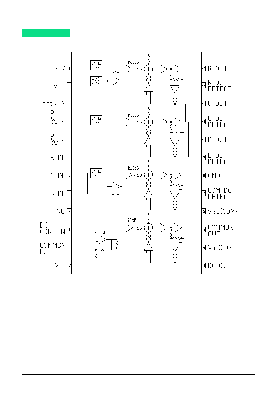
It has a built-in post filter (5MHzLPF), 16.5dB amp and 20dB common amp.
Features
1. Built-in post filter 5MHz LPF
2. Built-in amp G
V
=16.5dB
3. Adjustable white balance
4. Built-in common amp G
VCOM
=20dB
Package
SSOP-24 (0.8mm pitch)
TSOP-24 (0.5mm pitch)
Circuit Connection Diagram
Applications
1. Navigation systems
2. Digital cameras
3. Pachinko games (with color TFT)
4. Videophones, conferencing systems
5. Other game equipment
RGB signal after polarity inversion and
correction processing

MITSUMI
LCD Interface MM1323
Item
Symbol
Measurement conditions
Min. Typ. Max. Units
V
CC
1
4.8
4.9
5.0
V
Operating power supply voltage
V
CC
2
6.0
6.5
7.0
V
V
EE
-7.0 -6.5 -6.0
V
I
CC
1
No load
11.5 15.0 mA
Consumption current
I
CC
2
No load
8.5 11.0 mA
I
EE
No load
7.0
9.0 mA
RGB
R 16.0 16.5 17.0
Voltage gain
G
V
G 16.0 16.5 17.0 dB
B 16.0 16.5 17.0
Voltage gain difference
R-G -0.5 0.0
0.5
between channels
G
VCH
R-B -0.5 0.0
0.5
dB
G-B -0.5 0.0
0.5
Output dynamic range
V
ODR
V
P-P
R
2.3
2.5
2.7
Output center voltage
V
C
G
2.3
2.5
2.7
V
B
2.3
2.5
2.7
R
-0.2
0
0.2
Load fluctuation
V
OL
G -0.2
0
0.2
V
B -0.2
0
0.2
Frequency characteristic
F
C
W/B
R
1.5
V
P-P
Common-mode
V
W/BO
1
output amplitude
B
1.5
R
1.5
V
P-P
Negative-phase
V
W/BO
2
output amplitude
B
1.5
frpv input
V
T
1.0
1.7
2.4
V
threshold voltage
Common-
R
2.3
2.5
2.7
mode
B
2.3
2.5
2.7
Output center voltage
V
C
V
Negative-
R
2.3
2.5
2.7
phase
B
2.3
2.5
2.7
COMMON
COMMON voltage gain
G
VCOM
19.5 20.0 20.5 dB
COMMON output
V
CO
-0.2
0
0.2
V
center voltage
COMMON load fluctuation
V
OLC
-0.5
0
0.5
V
Center DC adjustment
Output voltage L
V
OL
SW5=B, V3=0V, Measure TP10 DC voltage.
-1.3 -1.0 -0.7
V
Output voltage H
V
OH
SW5=B, V3=3V, Measure TP10 DC voltage.
3.7
4.0
4.3
V
SW1, SW2, SW3=B V1, V2=1.5V
TP5, TP6, TP7=0.6V
P-P
, 100kHz sine wave
Measure sine wave ratio between input signal and TP12, 13 and 14
Measure voltage gain difference between each RGB
channel.
SW1, SW2, SW3=B V1, V2=1.5V
TP5, TP6, TP7=0.6V
P-P
100kHz sine wave
Vary input signal amplitude and measure TP12, 13
and 14 amplitude at the point where TP12, 13 and
14 signals start to saturate.
Input a 0.6V
P-P
, 7.86kHz rectangular wave to TP5, 6
and 7, and measure TP12, 13 and 14 center voltage.
Measure TP12, 13 and 14 DC voltage fluctuation
when TP12, 13 and 14 load current is varied from
0 ±6mA.
SW1, SW2, SW3=B V1, V2=1.5V
TP5, TP6, TP7=0.6V
P-P
sweep signal
For 100kHz, measure frequency when attenuated
-3dB relative to TP12, 13 and 14 signals.
TP1=5.0V
P-P
7.86kHz rectangular wave
Confirm that TP12 and 14 signals are in phase with
TP1, then measure amplitude.
TP1=5.0V
P-P
7.86kHz rectangular wave
Confirm that TP12 and 14 signals are reverse phase
from TP1, then measure amplitude.
Measure TP18 voltage, then impress that voltage on
TP18. Given V1=0V, add DC voltage to TP1. Raise
gradually from 0V and measure TP1 voltage when
TP14 voltage goes over 2.5V.
TP1=5.0V
P-P
7.86kHz rectangular wave
Adjust V1 and V2 within 0~1.5V (in
phase) and set TP12 and 14 amplitude at
1.5V. Measure TP12 and TP14 center
voltage.
Measure in the same way for V1 and V2
adjusted within 1.5~3.0V (reverse phase).
SW4=B TP9=1.0V
P-P
100kHz sine wave
Measure ratio of input signal and TP11 sine wave.
SW4=B TP9=1.0V
P-P
7.86kHz rectangular wave
Measure TP11 center voltage.
Measure TP11 DC voltage fluctuation when TP11 load
current is varied from 0 ±100mA.
Electrical Characteristics
(Except where noted otherwise, Ta=25∞C, V
CC
1=4.9V, V
CC
2=6.5V, V
EE
=-6.5V all SW ; A)
R 4.25
G 4.25
B 4.25
R
4.0
5.0
G
4.0
5.0
B
4.0
5.0


