
MITSUMI
Wide Discriminator MM1327
Wide Discriminator
Monolithic IC MM1327
Outline
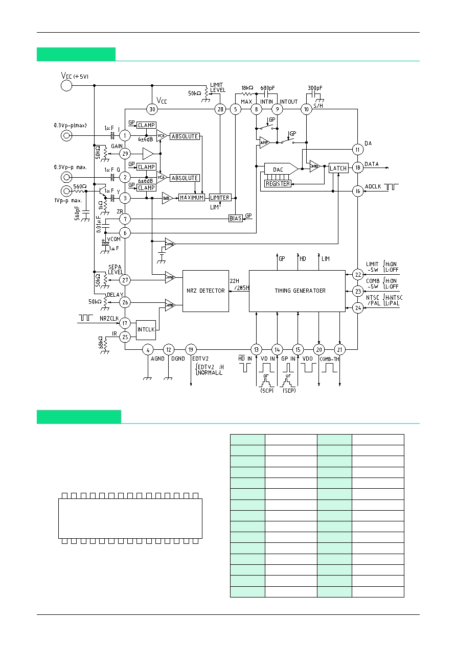
This IC identifies the letter box portion of wide broadcast, etc. video signals. The luminance and chroma
signals are used so that the rate of identification on dark screens is increased. Output is the total of 6bit ADC
data and character signal, etc. white peak signal discriminator bit, for 7bit data output.
In addition, an EDTV2 simple discrimination function is built-in.
Features
1. Signal level discrimination using composite luminance and chroma signal
2. Discrimination of video signal within horizontal scanning interval can be done every scan due to integrated
output
3. Built-in white peak detection circuit for subtitles
4. Built-in EDTV2 simple discrimination function
5. 22H discrimination output (COMB-THROUGH) circuit built-in
6. Built-in window limiter circuit
7. Data output is 7bit serial output format : 6bit ADC + peak detection
8. Operates on +5V single power supply
Package
SDIP-30
Applications
Wide TV
MITSUMI
Wide Discriminator MM1327
Block Diagram
Pin Assignment
SDIP-30
1
3
6
10
2
4 5
8
7
12
9
11
15
14
13
30
24
21
27
25
23 22
20
26
16
17
29 28
18
19
1
I
16
ADCLK
2
Q
17
NRZCLK
3
Y
18
DATA
4
AGND
19
EDTV2
5
MAX
20
VDO
6
VCOM
21
COMB-TH
7
ZR
22
LIMIT-SW
8
INT IN
23
COMB-SW
9
INT OUT
24
NTSC/PAL
10
S/H
25
IR
11
DA
26
DELAY
12
DGND
27
SEPA-LEVEL
13
HD
28
LIMIT-LEVEL
14
VD
29
GC
15
GP
30
V
CC
MITSUMI
Wide Discriminator MM1327
Pin Description
Pin no.
Pin name
Function
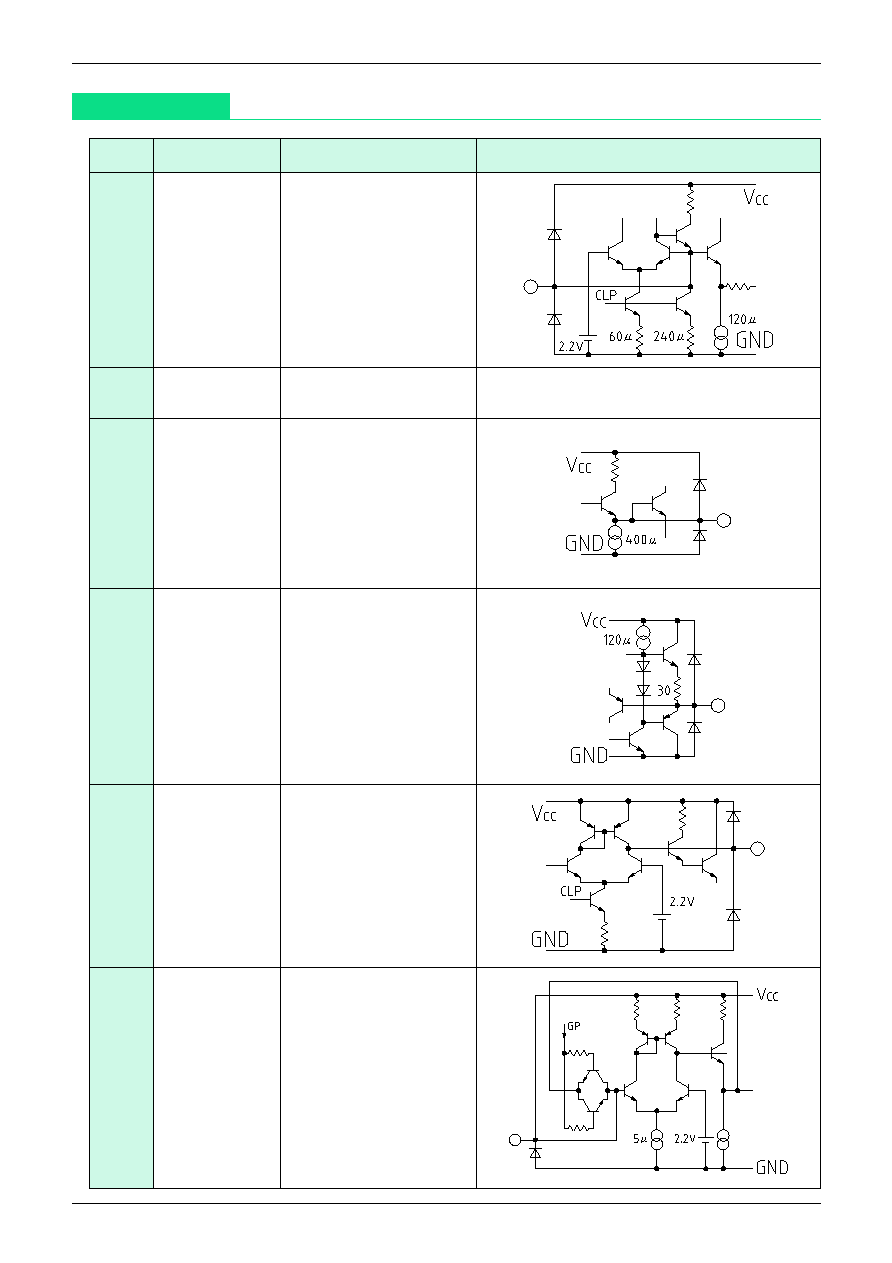
Internal equivalent circuit diagram
1
I
Video signal input pin
2
Q
3
Y
4
AGND
12
DGND
6
VCOM
7
ZR
8
INT IN
5
MAX
Composite output of input
video signal maximum
value
Internal reference voltage
output
Connect 1�F between this
pin and GND.
Connection pin for MAX
output clamp capacitor
Integrated circuit input pin
Integrated reset done at GP
timing.

MITSUMI
Wide Discriminator MM1327
Pin no.
Pin name
Function
Internal equivalent circuit diagram
9
INT OUT
10
S/H
11
DA
13
HD
--------------------------------------
IN
15
GP IN
14
VD IN
16
ADCLK
DAC output for consecutive
comparison ADC
Timing pulse input pins
GP operates even on SCP
input (5V
P-P
).
Timing pulse input pin
VD operates even on SCP
input (5V
P-P
).
Clock input pin for
consecutive ADC
Integrated output pin and
sample and hold pins
S/H of integration results
at HD timing
MITSUMI
Wide Discriminator MM1327
Pin no.
Pin name
Function
Internal equivalent circuit diagram
17
NRZCLK
25
IR
26
DELAY
18
DATA
19
EDTV2
20
VDO
21
COMB-TH
22
LIMIT-SW
23
COMB-SW
24
NTSC/PAL
27
SEPA LEVEL
28
LIMIT LEVEL
Switching pins
NRZ discrimination
luminance signal SEPA
level adjustment pin
MAX composite output
limit level adjustment pin
Limit area:
NTSC : 42~241H
PAL : 46~291H
Clock input pins for NRZ
discrimination
Input CLK is integrated by
resistor connected between
Pin 25 and GND and
internal 20pF, and delay is
set by Pin 26 voltage.
29
GAIN
I, Q gain adjustment pin
30
V
CC
Data output pins
MITSUMI
Wide Discriminator MM1327
Absolute Maximum Ratings
Item
Symbol
Ratings
Units
Operating temperature
T
OPR
-20~+75
�C
Storage temperature
T
STG
-40~+125
�C
Power supply voltage
V
CC
max.
7.0
V
Input voltage
V
IN
max.
GND <= V
IN
<
= V
CC
V
Allowable loss
Pd
800
mW
Recommended Operating Conditions
Item
Symbol
Ratings
Units
Operating temperature
T
OPR
-20~+75
�C
Operating voltage
V
OPR
4.5~5.5
V

MITSUMI
Wide Discriminator MM1327
Item
Symbol
Measurement conditions
Min. Typ. Max. Units
Consumption current
I
CC
20
30
mA
MAX amp
Y
V
YIN
*
1
2.0
2.2
2.4
Clamping level
I
V
IIN
*
1
2.0
2.2
2.4
V
Q
V
QIN
*
1
2.0
2.2
2.4
MAX output pin voltage
V max.
*
1
2.0
2.2
2.4
V
Y
V max.
Y
1.0
Maximum input level
I
V max.
I
0.6
V
P-P
Q
V max.
Q
0.6
Y input voltage gain
G
Y
*
2
-0.5
0.0
0.5
dB
Maximum gain
I
G max.
I
V
GC
=1.2V
*
3
+11.5 +12.0 +12.5
dB
Q
G max.
Q
V
GC
=1.2V
*
3
+11.5 +12.0 +12.5
Minimum gain
I
G min.
I
V
GC
=3.6V
*
3
-0.5
0.0
0.5
dB
Q
G min.
Q
V
GC
=3.6V
*
3
-0.5
0.0
0.5
I, Q gain difference
G
IQ
G
IQ
=G
I
-G
Q
-0.5
0.0
0.5
dB
EDTV II discrimination
NRZ detection level
L
V
YSL
5
7
IRE
H
V
YSH
27
30
NRZ detection readout timing
L
V
CSL
0.4
0.7
�S
H
V
CSH
1.5
1.8
NRZCLK pin input current
L
I
NRZCL
V
NRZCLK
=0.4V
1
�A
H
I
NRZCH
V
NRZCLK
=4.5V
1
IR pin voltage
V
IR
2.2
2.4
2.6
V
EDTV II output voltage L
V
NL
I
NL
=1mA
0.4
V
Trigger signal
HD
IN
V
THD
HD
2.30
2.50
2.70
Sync signal separation level
VD
IN
V
TVD
VD or SCP
0.63
0.83
1.03
V
GP
IN
V
TGP
GP or SCP
3.69
3.89
4.09
HD pin input current
L
I
HDL
V
HD
=0.4V
1
�A
H
I
HDH
V
HD
=4.5V
1
VD pin input current
L
I
VDL
V
VD
=0.4V
1
�A
H
I
VDH
V
VD
=4.5V
1
GP pin input current
L
I
GPL
V
GP
=0.4V
1
�A
H
I
GPH
V
GP
=4.5V
1
COMB-SW switching voltage
L
V
TCOSL
0.7
V
H
V
TCOSH
2.1
COMB-TH output voltage L
V
OCOMB
I
COMB
=1mA
0.4
V
VDO output voltage L
V
OVDO
I
VDO
=1mA
0.4
V
VCA
Electrical Characteristics
(Except where noted otherwise, Ta=25�C, V
CC
=5.0V)

MITSUMI
Wide Discriminator MM1327
Note 1 :
*
1 Clamp level and MAX output pin voltage
Measure voltage on each pin when GPIN and HDIN are connected to V
CC
.
Note 2 :
*
2 Y input voltage gain
Input a sweep signal to Y input, input a clamp pulse synchronized to H
SYNC
to GPIN pin, and
measure voltage gain at MAX pin for 100kHz.
Note 3 :
*
3 I, Q max/min gain
Input a square wave signal as shown below and a GPIN signal to I input (or Q input) and GPIN
pin, and measure voltage gain at MAX pin.
Note 4 :
*
4 MAX amp limit level
Measure limit level at MAX pin when LIMIT-SW pin is high. However, the limit range is as follows
for the NTSC/PAL pin.
Note 5 :
*
5 Offset voltage for reset
Connect GPIN pin to V
CC
and measure potential difference between INT IN pin and INT OUT pin.
Note 6 :
*
6 Integrated limit voltage
Input a 100% white signal to Y input and a clamp pulse synchronized to H
SYNC
to GPIN pin.
Measure INT OUT pin voltage at integration end at this time.
0.3V
0V
5V
0V
63.5
�
S
2
�
S
I or Q signal
GP pin
100IRE
Y input
INT OUT output
V
INTL

MITSUMI
Wide Discriminator MM1327
Timing Chart 1
259H
Composite
1st field
2nd field
SCP
GP
VB
RB
VDO
COMB-TB
25H
260H 261H 262H
1H
2H
3H
4H
5H
6H
7H
8H
9H
10H 11H 12H 13H 14H 15H 16H 17H 18H 19H 20H 21H 22H 23H 24H
-5V
-5V
-5V
-5V
-2.8V
-1.7V
-0V
-0V
-0V
-0V
260H
Composite
1st field
2nd field
SCP
GP
VB
RB
VDO
COMB-TB
25H
261H 262H 263H
1H
2H
3H
4H
5H
6H
7H
8H
9H
10H 11H 12H 13H 14H 15H 16H 17H 18H 19H 20H 21H 22H 23H 24H
-5V
-5V
-5V
-5V
-2.8V
-1.7V
-0V
-0V
-0V
-0V

MITSUMI
Wide Discriminator MM1327
Timing Chart 2
50IRE
0IRE
50IRE
100IRE
Y input
I (Q) input
MAX output
tegrated output
S/H
GP
HD
ADCLX
DATA
PEAK 05
00
+0.15V
-0.15
3FM
00M
1. The largest of Y, I and Q video input signals is output on MAX output pin.
2. MAX output date is integrated during horizontal scanning.
3. Integration results are sampled and held at HD pulse timing.
4. Consecutive comparison ADC outputs data as serial data.
(Serial data is 1H delayed from video signal input.)
5. Output data configuration is as shown in the table below.
Data configuration
Video
DATA
White scanning
00
Black scanning
3F
Y input
PEAK
Peak of more than 50IRE
1
No peak of more than 50IRE
0
Timing Chart 3
1
0
1
1
0
DELAY
Y
IN
(22H)
NRZCLK
Integrated NRZCLK
NRZ discrimination timing
(Internal circuit)
1. When Y
IN
input signal matches "10110" at NRZ discrimination timing, it is identified as an EDTV2 signal.
EDTV2 pin is high for EDTV2 identification.
MITSUMI
Wide Discriminator MM1327
Measuring Circuit