 | –≠–ª–µ–∫—Ç—Ä–æ–Ω–Ω—ã–π –∫–æ–º–ø–æ–Ω–µ–Ω—Ç: MM1333 | –°–∫–∞—á–∞—Ç—å:  PDF PDF  ZIP ZIP |
MITSUMI
Control for Lithium Ion Battery Charging (one cell) MM1333
Control for Lithium Ion Battery Charging (one cell)
Monolithic IC MM1333
Outline
This IC was developed for use in charging lithium ion batteries. PNP power transistor or P-MOS FET is
mounted externally to control charging. This IC is for use with a single cell only, and provides precise control
of the charging voltage ; the charging current can be set through an external resistance. In addition to the
functions of the MM1332, it incorporates a comparator for full-charge detection.
Features
1. Output voltage 1 (Ta=25∞C)
4.100V±35mV
2. Output voltage 2 (Ta=0∞C~+40∞C)
4.100V±50mV
3. Constant-current output
Current limit
100mV±10mV
Constant current value = current limit/external resistance
4. Low-voltage (LV) detection function
2.00V±100mV
5. Full-charge detection function
Detection voltage
31mV±5mV
Package
VSOP-8A (MM1333 W)
Note: Output (charge) voltage rank is inside the .
Applications
1. Lithium ion battery chargers
MITSUMI
Package
VSOP-8A, 8B
DW
4.200±0.050
D
20±3
1cell
MM1333
HW
4.100±0.050
D
31±5
1cell
JW
4.200±0.050
D
31±5
1cell
Output
voltage (V)
Output voltage
temperature
conditions
Full charge
detection
voltage (mV)
Over voltage
detection
voltage (v)
Remarks
*
Series Table
Temperature conditions A: Ta=-25~75∞C, B: Ta=-20~70∞C, C: Ta=0~50∞C,
D: Ta=0~40∞C
Note: In the case of rank D, the Co output voltage level changes to "L" when charging is turned ON. (The
function is reversed in the case of ranks H and J).
MITSUMI
Control for Lithium Ion Battery Charging (one cell) MM1333
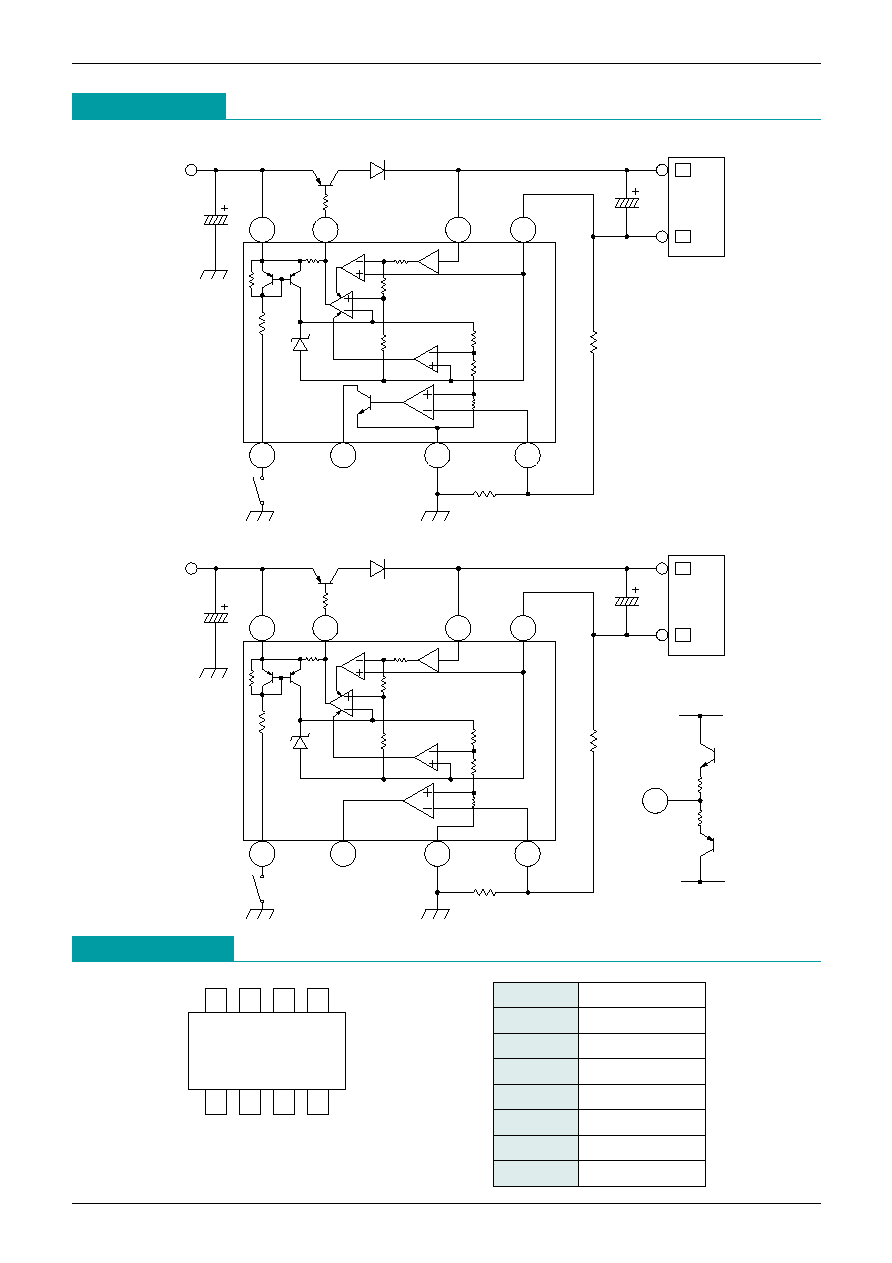
Pin Assignment
1
4
3
2
8
5
6
7
SOP-8C
SOP-8E
VSOP-8A
1
SW
2
CO
3
GND
4
CS2
5
CS1
6
CEL
7
EXT
8
V
CC
Block Diagram
1
8
7
6
5
2
3
4
+B
-B
BATTERY
PACK
R3
R4
0.10V
0.031V
J:4.2V
H:4.1V
2V
1.2V
BUF
1
8
7
6
5
2
3
4
+B
-B
BATTERY
PACK
R3
R4
0.10V
0.020V
BUF
D:4.2V
2V
V
CC
C
O
2
C
O
Pin Part
200
GND
200
2
1.2V
MM1333J, H
MM1333D
MITSUMI
Control for Lithium Ion Battery Charging (one cell) MM1333
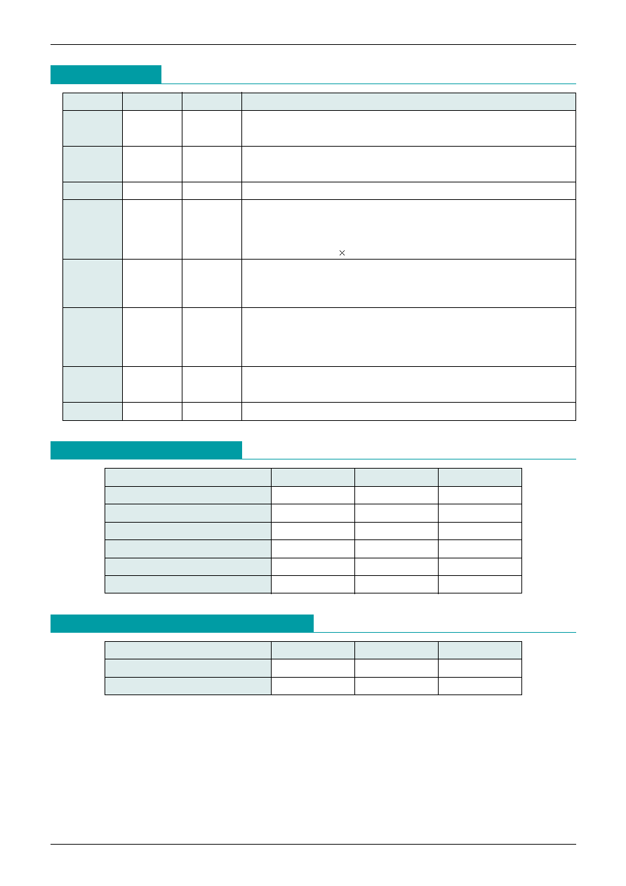
Recommended Operating Conditions
MITSUMI
Item
Symbol
Ratings
Units
Operating temperature
T
OPR
-20~+70
∞C
Operating voltage
V
OPR
+5~+12
V
Absolute Maximun Ratings
(Ta=25∞C)
Item
Symbol
Ratings
Units
Storage temperature
T
STG
-40~+125
∞C
Operating temperature
T
OPR
-20~+70
∞C
Power supply voltage
V
CC
max.
-0.3~+13
V
Output voltage
V
O
max.
-0.3~V
CC
V
SW input voltage
V
SW
-0.3~V
CC
+0.3
V
Allowable loss
Pd
300
mW
Pin Description
Values given are standard
Pin no.
Pin name
Input/output
Function
1
SW
Input
Input pin for on/off control
SW=V
CC
: off, SW=GND : on
Pulled up to V
CC
, so turned off when open
Full-charge signal output pin
While charging : Open collector output NPN transistor is off
At full charge : Open collector output NPN transistor is on
2
CO
output
GROUND pin
3
GND
Input
Full charge detection pin
The current is detected through the voltage drop across an external
resistance, to control the full-charge signal.
The ratio of the charge current set by CS1 and the current at full-charge signal
output is (VIC)/(0.1 V R4/(R3+R4))
4
CS2
Input
Current detection pin
The current is detected through the voltage drop across an external
resistance, to maintain a constant current. The current value can be set using
0.1 V/(R3+R4).
5
CS1
Input
6
CEL
Input
Battery voltage input pin
The battery voltage is detected and used to maintain the voltage at the
prescribed value.
A low-voltage detection circuit is also present, and charging is forbidden when
the battery voltage is less than 2V.
Constant-voltage circuit output pin
The base of an external PNP transistor or gate of a P-MOS FET is controlled in
constant-voltage charging.
7
EXT
Output
8
V
CC
Input
Power supply input pin

MITSUMI
Control for Lithium Ion Battery Charging (one cell) MM1333
Measurement Method
(Except where noted otherwise, Ta=25∞C, V
CC
=5V, SW2 : A, SW4 : A, SW6 : A, SW7 : A)
MITSUMI
Item
Measurement Method
Consumption current 1
Set V1=0 V, SW4=B, V4=50mV, V6=4.5V ; switch SW6 from A to B and again to A ; then measure the A8 current I
CC
1.
Consumption current 2
Set V1=0V, SW4=B, V4=50mV, V6=4.5V ; switch SW6 from A to B and again to A ; then measure the A8 current I
CC
1.
Consumption current 3
Set V1=V
CC
, and measure the resulting A8 current I
CC
3.
Output voltage
Set V1=0V, V6=4.5V; switch SW6 from A to B and again to A ; then measure the T6 voltage V
O
.
Current limit
Set V1=0V, set the voltage V6 about 1V lower than the potential at T6 (output voltage), and set SW6
to B ; then measure the T5 voltage V
CL
.
CEL-CS leakage current
Set V
CC
=0V, V1=0V; set the voltage V6 to 5V; and set SW6 to B and SW7 to C. Then measure the A6 current I
CEL
.
SW input current
With V1=0V, measure the A1 current I
SW
1.
SW input voltage
Set the voltage V6 1V lower than the T6 potential (output voltage), and set SW6 to B. With the
voltage V1 variable, when the A6 current is 100mA or higher this voltage is equal to the charge-on
voltage (VL), and when the current is within ±10µA it is equal to the charge-off voltage (VH).
Low-voltage
detection voltage
Set V1=0 V, set V6 to 1V lower than the T6 potential (output voltage), and set switch SW6 to B. Then
gradually lower the voltage V6 ; the voltage V6 at which the A6 current is within ±10µA is LV.
EXT pin input voltage
Measure the A7 current IS with V1=0V, SW6 set to B, SW7 set to B, V6=3V, and V7=4V.
EXT pin output voltage
Set V1=0 V, SW6 to B, and SW7 to C. The T7 voltage when V6=3V and V6=5V is V
EXT
.
Full-charge
detection voltage
Set V1=0V and SW4 to B. Gradually lower the voltage V4 from 50mV ; the voltage V4 when the T2
potential falls to 1V or lower from (V
CC
-1) V or higher is VIC.
Full-charge
detection output L
Measure the T2 voltage V
COL
when V1=0V, SW4 is at B and V4=0V.
Full-charge detection
output leakage current
Measure the A2 current I
CO
when V1=0V, SW4 is at B, V4=50mV, SW2 is at B, and V2=5V.
Warnings regarding use
1. The following components should be added in preparation for use.
1. A capacitance of several µF or so between V
CC
and GND
2. A 10µF capacitor between CEL and CS
3. A diode to prevent backflow between the collector of the external PNP transistor and pin 6
4. A current-limiting 150
resistor between the base of the external PNP transistor and EXT
2. The full charge detection circuit detects voltages of order several mV, and so no hysteresis is applied.
Chattering will occur, and should be born in mind.
3. There is an internal low-voltage detection circuit. If a voltage of at least 2V is not applied to the CEL pin, no
output will be obtained.
Electrical Characteristics
(Except where noted otherwise, Ta=25∞C, V
CC
=5V, SW2, 4, 6, 7 : A) Models listed MM1333
Item
Symbol
Measurement conditions
Min. Typ. Max. Units
Consumption current 1
I
CC
1
VSW=0V (Charge : ON)
300
400
µA
Consumption current 2
I
CC
2
VSW=0V (Charge : ON)
1.1
1.6
mA
Consumption current 3
I
CC
3
VSW=V
CC
(Charge : OFF)
2
4
µA
Output voltage 1
V
O
1
Ta=25∞C
4.065 4.100 4.135
V
Output voltage 2
V
O
2
Ta=0~+40∞C
4.050 4.100 4.150
V
Output voltage temperature drift
V
O
Ta=-20~+70∞C
±0.25
mV
∞C
Current limit
V
CL
90
100
110
mV
CEL-CS leakage current
I
CEL
1
µA
SW input current
I
SW
20
µA
SW input voltage
V
L
Charge : ON
-0.3
2.0
V
V
H
Charge : OFF
V
CC
-1.0
V
CC
+0.3
V
Low-voltage detection voltage
L
V
1.90
2.00
2.10
V
EXT pin input voltage
I
S
10
20
mA
EXT pin output voltage
V
EXT
No load
0.3
V
CC
-0.3
V
Full-charge detection voltage
V
IC
26
31
36
mV
Full-charge detection output L
V
COL
I
SINK
=0.3mA
0.2
0.4
V
Full-charge detection
output leakage current
I
CO
1
µA
MITSUMI
Control for Lithium Ion Battery Charging (one cell) MM1333
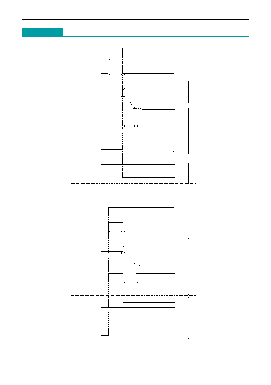
Timing Chart
V
CC
OFF
OFF
ON
ON
(V
CC
- 1.0 ~ V
CC
+ 0.3)
V
H
SW
CEL
CS1,2
(When R3=0)
Battery connected and SW on
CS1,2
(When R3=0)
CO
CO
CEL
Charge off
Charge off
Charge on signal
With CO pulled up to V
CC
by a resistance
Full-charge signal
Charge on
Normal charging
Low battery voltage
(2V or lower)
V
L
(-0.2~2.0V)
0
0
100mV
0
0
0
0
0
H
H
L
L
31mV
Note: In the case of rank D, the Co output voltage level changes to "L" when charging is turned ON. (The
function is reversed in the case of ranks H and J).
V
CC
OFF
SW
Battery connected and SW ON
0
0
OFF
ON
ON
CEL
CS1,2
(When R3=0)
CS1,2
(When R3=0)
CO
CO
CEL
Charge OFF
Charge OFF
Charge ON signal
Full-charge signal
Charge ON
Normal charging
Low battery voltage
(2V or lower)
0
100mV
0
0
0
0
0
H
L
20mV
H
MM1333J, H
MM1333D
MITSUMI
Control for Lithium Ion Battery Charging (one cell) MM1333
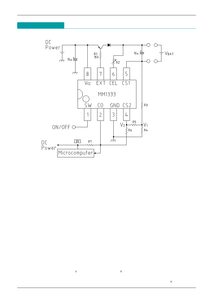
Application circuits
1. A diode is required to prevent reverse current from the battery.
2. Even higher precision can be obtained by inserting R2 for output voltage adjustment.
CEL intake current is used to adjust output voltage with R2. CEL intake current is around 3 ~ 10µA.
3. Charging current can be set with R3+R4.
Example : To set to 0.25A
VCL/(R3+R4) = 0.1V/0.4
= 0.25A
4. Full charge detection current can be adjusted by the ratio between R3 and R4.
Example : H rank
VIC/(VLC R4/(R3 + R4) = 0.031V/(0.1 0.21
/(0.19 + 0.21)) = 0.59
This makes the ratio between charging current and full charge detection current 1 : 0.59.
Charging current was set at 0.25A in step 3 above, so full charge detection current is 0.25A 0.59 = 0.148A.

MITSUMI
Control for Lithium Ion Battery Charging (one cell) MM1333
5. R5 and R6 are resistors for positive feedback (hysteresis). Hysteresis is applied for the amount of R5
voltage drop, and should be set below (about 1/3) full charge voltage.
Also, at this time, full charge detection voltage changes by the amount of R5 voltage drop.
Example : Setting full charge detection current using H rank and taking hysteresis voltage into account.
Setting conditions : charge current 0.25A (R3 + R4=0.4
), full charge current 0.1A, MPU power supply 5V,
full charge hysteresis 10mV
Full charge current is set by comparing the reference voltage (VIC=0.031V) and CS2 pin voltage (V2) inside
the IC. An example of calculation for setting full charge current at 0.1A is shown below.
(V2-V1)+IBATT R4=0.031V
Here, V2-V1 (potential at ends of R5) is the hysteresis. In order to set hysteresis at 10mV, find R4 as
follows.
R4=(0.031V-(V2-V1)/IBATT=(0.031V-0.01V)/0.1A = 0.21
From R3 + R4 = 0.4
, R3 = 0.4-0.21 = 0.19.
Hysteresis Setting (R5 ~ R7)
The current values that flow on R5~R7 from 3V are minute due to the high impedance of the CS2 pin, and
so do not cause a problem. (It is assumed that the effects of noise, etc. must be considered for each
individual set.) Here the setting is for 10µA. CO is low level during full charge detection, so V2-V1 = 0V.
When V2-V1 is set to 10mV during charging (CO high), then R5 + R6 + R7 = 3V/10µA = 300kW. (R4 is
extremely small as compared to R5~R7 and thus is ignored.)
3V : 0.01V=(R5 + R6 + R7) : R5
From the above equation, R5 = 1k
, R6 + R7 = 299k, and R6 and R7 resistance values must be set so
that CS1 can be low level. If CS1 sink current is 0.15mA, then R7 = 3V/0.15mA=20k
, R6=299k-20k =
279k
.
Therefore, R3 = 0.19
, R4 = 0.21, R5 = 1k, R6 = 279k, R7 = 20k.
Please note that the above figures are examples given for reference purposes, and should be used in actual
practice only after sufficient examination.

MITSUMI
Control for Lithium Ion Battery Charging (one cell) MM1333
Charging (V
CC
=5V, Output voltage 4.1V)
Output voltage vs ambient temperature
(V
CC
=5V, Output voltage 4.1V)
Output voltage vs power supply voltage
(Ta=25∞C, Output voltage 4.1V)
4.15
4.14
4.13
4.12
4.11
4.1
4.09
4.08
4.07
4.06
4.05
Output voltage (V)
-25
0
25
50
75
Ambient temperature (
∞C)
4.15
4.14
4.13
4.12
4.11
4.1
4.09
4.08
4.07
4.06
4.05
5 6 7 8 9 10 11 12 13 14 15 16 17 18
Power supply voltage (V)
Output voltage (V)
4.5
4.4
4.3
4.2
4.1
4
3.9
3.8
3.7
3.6
3.5
Power supply voltage V (V)
0
0.5
1
1.5
2
2.5
3
Charging time (h)
Characteristics
MITSUMI
35
30
25
-25
25
75 85
Ambient temperature (
∞C)
H-rank full charge detection voltage (mV)
25
20
15
-25
25
75 85
Ambient temperature (
∞C)
D-rank full charge detection voltage (mV)
H-rank full charge detection voltage [mV]
D-rank full charge detection voltage [mV]
0
5
10
15
20
4.15
4.10
4.05
Power supply voltage (V)
H-rank output voltage (V)
H-rank output voltage [V]
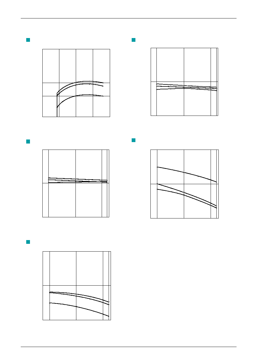
MITSUMI
Control for Lithium Ion Battery Charging (one cell) MM1333
0
5
10
15
20
4.25
4.20
4.18
4.15
Power supply voltage (V)
D-rank output voltage(V)
-25
25
75 85
2.1
2.0
1.9
Ambient temperature (
∞C)
Low-voltage detection voltage (V)
-25
25
75 85
110
100
90
Ambient temperature (
∞C)
CS1 pin voltage (mV)
25
-25
75 85
4.15
4.10
4.05
Ambient temperature (
∞C)
H-rank output voltage(V)
-25
25
75 85
4.25
4.20
4.15
Ambient temperature (
∞C)
D-rank output voltage(V)
D-rank output voltage [V]
Low-voltage detection voltage [V]
CS1 pin voltage [V]
H-rank output voltage
[
V
]
D-rank output voltage
[
V
]