 | –≠–ª–µ–∫—Ç—Ä–æ–Ω–Ω—ã–π –∫–æ–º–ø–æ–Ω–µ–Ω—Ç: MM1377 | –°–∫–∞—á–∞—Ç—å:  PDF PDF  ZIP ZIP |

MITSUMI
Voltage and Current Control (dual op-amp and shunt regulator) (quad op-amp and shunt regulator) MM1377, 1378
Voltage and Current Control
(dual op-amp and shunt regulator) (quad op-amp and shunt regulator)
Monolithic IC MM1377, 1378
Outline
The MM1377 incorporates an op-amp with a dual low-input offset voltage and a shunt regulator; the MM1378
combines a quad low-input offset voltage op-amp and shunt regulator. They are appropriate for use in battery
chargers, switching power supplies and other voltage and current control applications. Op-amps with low input
offset voltage are particularly well-suited for handling current detection signals and other low-amplitude signals.
Features
Op-amp unit
1. Input offset voltage
0.2mV typ.
2. Input offset current
5nA typ.
3. Input bias current
30nA typ.
4. Common-mode input voltage range
0~V
CC
-1V
5. Power supply current
0.6mA typ.
Shunt regulator unit
1. Reference voltage
2.5V typ.
2. Reference voltage fluctuation (-20~+80∞C)
5mV typ.
3. Minimum cathode current
0.4mA typ.
Package
SOP-8C, SOP-8E (MM1377)
SOP-14B (MM1378)
Applications
1. Charger
2. Switching power supply
3. AC adapter
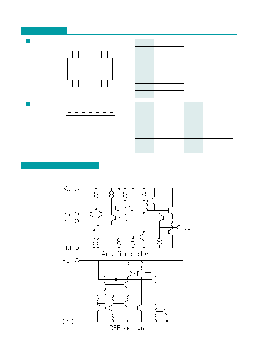
Block Diagram
MM1377
MM1378
MITSUMI
Voltage and Current Control (dual op-amp and shunt regulator) (quad op-amp and shunt regulator) MM1377, 1378
Equivalent Circuit Diagram
Pin Assignment
1
4
3
2
8
5
6
7
SOP-8C, SOP-8E
1
A
OUT
2
A
IN-
3
A
IN+
(REF)
4
GND
5
B
IN+
6
B
IN-
7
B
OUT
8
V
CC
SOP-14B
1
3
6
2
4
5
7
14
11
9
13 12
10
8
1
A
OUT
8
C
OUT
2
A
IN-
9
C
IN-
3
A
IN+
(REF)
10
C
IN+
4
V
CC
11
GND
5
B
IN+
12
D
IN+
6
B
IN-
13
D
IN-
7
B
OUT
14
D
OUT
MM1377
MM1378

MITSUMI
Voltage and Current Control (dual op-amp and shunt regulator) (quad op-amp and shunt regulator) MM1377, 1378
Absolute Maximun Ratings
Item
Symbol
Ratings
Units
Storage temperature
T
STG
-40~+125
∞C
Operating temperature
T
OPR
-20~+85
∞C
Power supply voltage
V
CC
max.
-0.3~+24
V
Allowable loss
P
D
300 (MM1377)
mW
350 (MM1378)
Recommended Operating Conditions
Item
Symbol
Ratings
Units
Operating temperature
T
OPR
-15~+80
∞C
Operating voltage
V
OPR
+2~+20
*
V
Electrical Characteristics
(Except where noted otherwise, V
CC
=5V, Ta=25∞C)
Item
Symbol
Measurement conditions
Min. Typ. Max. Units
Op-amp unit
Input offset voltage
V
IO
0.2
0.9
mV
Input offset current
I
IO
Excluding amp A
5
50
nA
Input bias current
I
B
30
150
nA
Common-mode input voltage range
V
I
Excluding amp A
0
V
CC
-1
V
Power supply current
I
CC
R
L
=
, for two circuits
MM1377
0.6
1.0
mA
R
L
=
, for four circuits
MM1378
1.2
2.0
Voltage gain
A
V
100
dB
Output voltage L
V
OL
R
L
=
10
100
mV
Output voltage H
V
OH
R
L
=
V
CC
-1.1 V
CC
-0.8
V
Common-mode signal rejection ratio
CMRR
65
85
dB
Power supply voltage rejection ratio
PSRR
65
100
dB
Output outflow current
I
SO
20
35
mA
Output inflow current
I
SI
10
20
mA
Shunt regulator
Reference voltage
V
REF
2.450 2.500 2.550
V
Reference voltage fluctuation
V
REF
5
17
mV
within operating temperature range
Minimum cathode current
I min.
0.4
1.0
mA
Dynamic impedance
Z
KA
0.4
0.7
*
Minimum value of operating voltage is for amp unit only
2
1.5
1
0.5
0
0
5
10
15
20
25
30
Power supply voltage (V)
Op-amp unit
consumption current
(
mA
)
MM1378
MM1377
MITSUMI
Voltage and Current Control (dual op-amp and shunt regulator) (quad op-amp and shunt regulator) MM1377, 1378
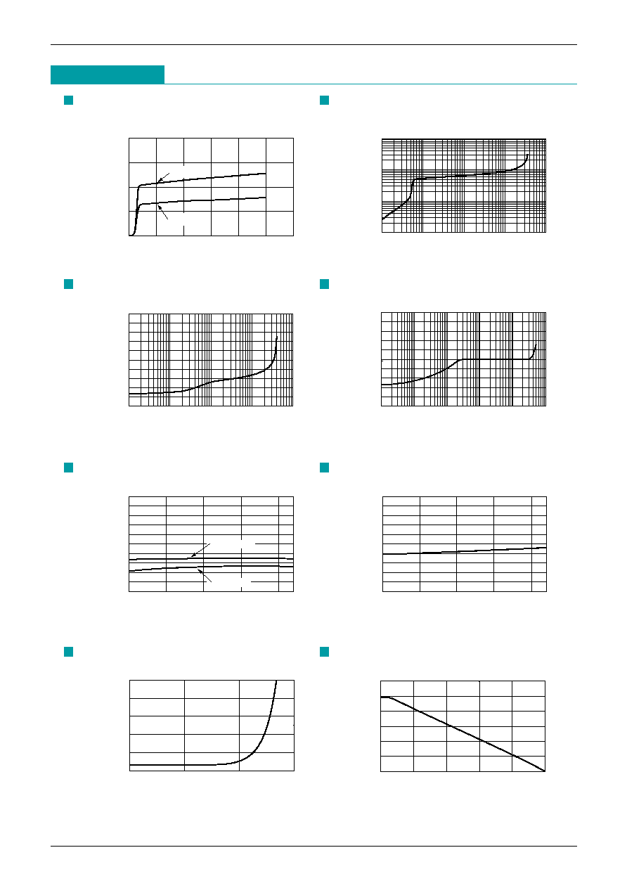
Characteristics
Consumption current vs power supply voltage
(Ta=25∞C)
10
1
0.1
0.01
0.01
0.1
1
10
100
Output voltage
(
V
)
Sync current (
mA)
Output voltage vs sync current (Ta=25∞C)
5
4
3
2
1
0
0.01
0.1
1
10
100
Source current (mA)
V
CC
-output
voltage
(
V
)
(V
CC
-output voltage) vs source current (Ta=25∞C)
5
4
3
2
1
0
0.001
0.01
0.1
1
10
100
Cathode current (mA)
Reference voltage
(
V
)
Reference voltage vs cathode current (Ta=25∞C)
2.55
2.5
2.45
-25
0
25
50
75
Reference voltage
(
V
)
Ambient temperature (
∞
C)
Ik = 20mA
Ik = 1mA
Reference voltage vs Ambient temperature
1
0.8
0.6
0.4
0.2
0
-0.2
-0.4
-0.6
-0.8
-1
-25
0
25
50
75
Input offset voltage
(
mV
)
Ambient temperature (
∞
C)
Input offset voltage vs Ambient temperature
5
4
3
2
1
0
1k
10k
100k
1M
Dynamic impedance (
)
Frequency (Hz)
Dynamic impedance vs frequency (Ta=25∞C)
120
100
80
60
40
20
0
0
100
1k
10k
100k
1M
Voltage gain (dB)
Frequency (Hz)
Voltage gain vs frequency (Ta=25∞C)