 | ÐлекÑÑоннÑй компоненÑ: MM1454 | СкаÑаÑÑ:  PDF PDF  ZIP ZIP |
Äîêóìåíòàöèÿ è îïèñàíèÿ www.docs.chipfind.ru

MITSUMI
Q Surround Processor MM1454
Q Surround Processor
Monolithic IC MM1454
Outline
This is an analog IC virtual surround processor that faithfully reproduces the sound algorithm developed by Q
SOUND Labs, Inc.
In particular, when a stereo signal (L/Rch) encoded by Dolby Pro Logic is input to this IC, a virtual rear speaker
is created spatially, and this allows reproduction of realistic, 3-dimensional sound from two speakers, without
the addition of another speaker.
Q Xpander technology allows deep, spatially wide sound for input of normal stereo signals, as well.
*
Virtual Dolby sound is a system developed by Dolby Labs, Inc. that reproduces realistic Pro Logic sound
with just two front left and right speakers, so there is no need for the additional two rear speakers and
center speaker normally required for Pro Logic sound.
*
Dolby and Dolby Surround are registered trademarks of Dolby Laboratory Licensing Corporation.
*
The Q Surround virtual processor (MM1454) was developed by Mitsumi Electric, and has not received the
certification or authorization of Dolby Laboratory.
*
Mitsumi Electric has no business ties or other relationship with Dolby Laboratory.
Features
Package
1. Virtual rear speakers allow reproduction of 3-dimensional sound through only two speakers when a Pro
Logic encoded source is input.
2. Also reproduces wide sound for a normal stereo source.
3. 2ch input - 2ch output.
4. Few external parts due to use of the active filter created using Mitsumi's bipolar technology.
5. Low noise design
Q Surround
ON: 15µVrms
OFF: 10µVrms
6. Simple structure results in small size and low cost.
SOP-16B
Item
Symbol
Rating
Unit
Storage Temperature
T
STG
-40~+125
°C
Operating Temperature
T
OPR
-20~+75
°C
Power Supply Voltage
V
CC
max.
13
V
Input Voltage
V
IN
max.
0 <
= V
IN
<
= V
CC
V
Output Voltage
I
O
max.
10
mA
Allowable loss
Pd
350
mW
Absolute Maximum Ratings
(Ta=25°C)
Applications
1. TV, VCR
2. Audio equipment
3. Computer monitors
4. Active speaker systems

MITSUMI
Q Surround Processor MM1454
Recommended Operating Conditions
Electrical Characteristics
(Except where noted otherwise, V
CC
=9V, Ta=25°C, Vbyp=5V, SW1,2,3: A)
Item
Symbol
Rating
Unit
Operating temperature
T
OPR
-20~+75 °C
Operating voltage
V
OP
4.5~12.0
V
Power supply fall times
*
7
T
VOFF
0.1~1.0
S
Item
Symbol
Measurement Conditions
Min. Typ. Max. Unit
Current consumption
I
CC
16
22
mA
Voltage gain Q Surround 1
Gqs1
SG1 : 0.75Vrms, 1kHz SW2 : B
TP1
8.5
9.5
10.5
dB
Voltage gain Q Surround 2
Gqs2
SG1 : 0.75Vrms, 1kHz SW2 : B
TP2
4.0
5.0
6.0
dB
Voltage gain Q Surround 3
Gqs3
SG2 : 0.75Vrms, 1kHz SW3 : B
TP2
8.5
9.5
10.5
dB
Voltage gain Q Surround 4
Gqs4
SG2 : 0.75Vrms, 1kHz SW3 : B
TP1
4.0
5.0
6.0
dB
Voltage gain bias 1
Gby1
SG1 : 0.75Vrms, 1kHz
Vbyp=0V
-1
0
1
dB
SW2 : B
TP1
Voltage gain bias 2
Gby2
SG2 : 0.75Vrms, 1kHz
Vbyp=0V
-1
0
1
dB
SW3 : B
TP2
Input voltage amplitude (1)
V
IN
1
V
CC
=9V
*
1 SW2, 3 : B
TP1, TP2
0.75
0.9
Vrms
Input voltage amplitude (2)
V
IN
2
V
CC
=9V
*
2 SW2, 3 : B
TP1, TP2
0.35
0.45
Vrms
Total higher harmonic
THDqs
(a) SG1 : 0.75Vrms, 1kHz SW2 : B
0.1
0.3
%
distortion Q Surround
(b) SG2 : 0.75Vrms, 1kHz SW3 : B TP1, TP2
Total higher harmonic
(a) SG1 : 0.75Vrms, 1kHz SW2 : B
distortion bias
THDby
(b) SG2 : 0.75Vrms, 1kHz SW3 : B
0.03
0.15
%
Vbyp=0V
TP1, TP2
Output noise voltage Q Surround
Vnoqs
BW=20~20kHz, A Curve
TP1, TP2
15
35
µVrms
Output noise voltage bias
Vnoby
BW=20~20kHz, A Curve
10
25
µVrms
Vbyp=0V
TP1, TP2
R-L channel balance
Cb
SG1, SG2 : 0.75Vrms, 1kHz
-1.0
0
1.0
dB
Vbyp=0V SW2, 3 : B
TP1, TP2
B/Q pin voltage (H)
Vbyph
*
3
2.1
V
B/Q pin voltage (L)
Vbyp1
*
4
0.7
V
B/Q pin voltage (H)
Ibyph
*
5 Vbyp=5V
TP5
350
µA
B/Q pin voltage (L)
Ibyp1
*
6 Vbyp=0V
TP5
-1
µA
DET pin voltage (H)
Vdeth
*
7
TP6
8.5
V
DET pin voltage (L)
Vdetl
*
7
TP6
0.7
V
Input resistance
R
IN
TP3, TP4
21
30
39
k
Power supply voltage
PSRRqx
SG3 : 100mVrms, 100Hz SW1 : B TP1, TP2
-80
-65
dB
removal rate Q Surround
Power supply voltage
PSRRby
SG3 : 100mVrms, 100Hz SW1 : B
-85
-70
dB
removal rate bias
Vbyp=0V
TP1, TP2
Crosstalk (1)
Ct1
SG1 : 0.75Vrms, 1kHz SW2 : B
-85
-70
dB
*
8 Vbyp=0V
TP1, TP2
Crosstalk (2)
Ct2
SG2 : 0.75Vrms, 1kHz SW3 : B
-85
-70
dB
*
9 Vbyp=0V
TP1, TP2

MITSUMI
Q Surround Processor MM1454
Note 1:
*
1 Input voltage amplitude when output total higher harmonic distortion is 1%. However, the signals
input to SG1 and SG2 must be the same phase (phase difference 0 degrees).
Note 2:
*
2 Input voltage amplitude when f = 1kHz and output total higher harmonic distortion is 1%. However,
the signals input to SG1 and SG2 must be reverse phase (phase difference 180 degrees).
Note 3:
*
3 Voltage when B/Q pin (Pin 3) is considered to be H (Q Surround mode).
Note 4:
*
4 Voltage when B/Q pin (Pin 3) is considered to be L (by pass mode).
Note 5:
*
5 Current that flows in to B/Q pin (Pin 3) when Vbyp = 5V.
Note 6:
*
6 Current that flows out of B/Q pin (Pin 3) when Vbyp = 0V.
Note 7:
*
7 The mute signal for turning off the power amp power supply is output to Pin 4. On this IC, it is
recommended that the pop noise generated during power supply fall be muted by turning off the
power amp connected to the final stage of MM1454 before turning off the IC power supply.
Note 8:
*
8 Defined as the ratio between Pin 6 output signal and Pin 7 output signal when a signal is input to
SG1.
Note 9:
*
9 Defined as the ratio between Pin 7 output signal and Pin 6 output signal when a signal is input to
SG2.
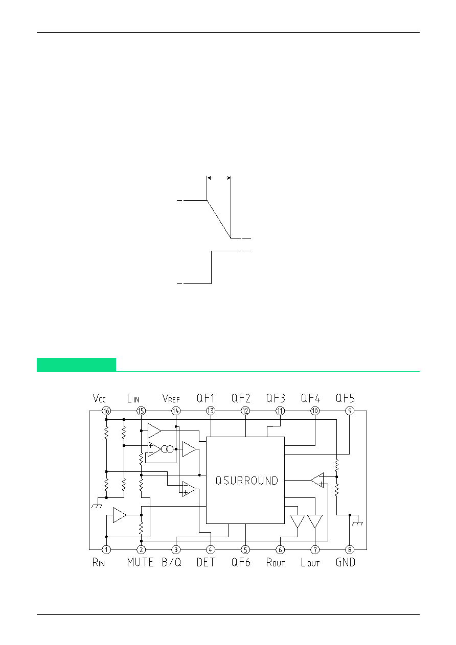
V
CC
=9V
Vdet 1
0V
Vdeth
V
CC
waveform (16PIN)
DET pin waveform (4PIN)
Tvoff
Block Diagram

MITSUMI
Q Surround Processor MM1454
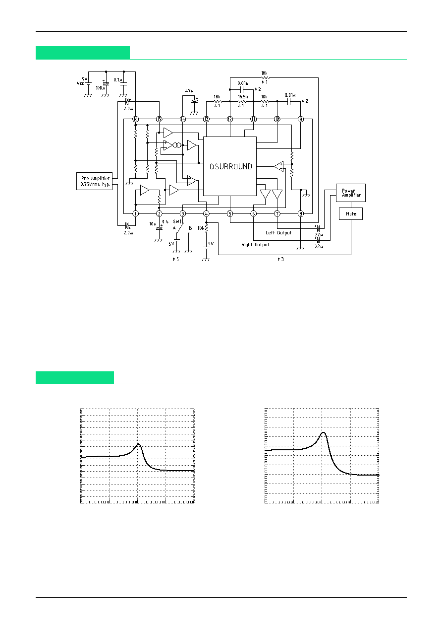
Application Circuit
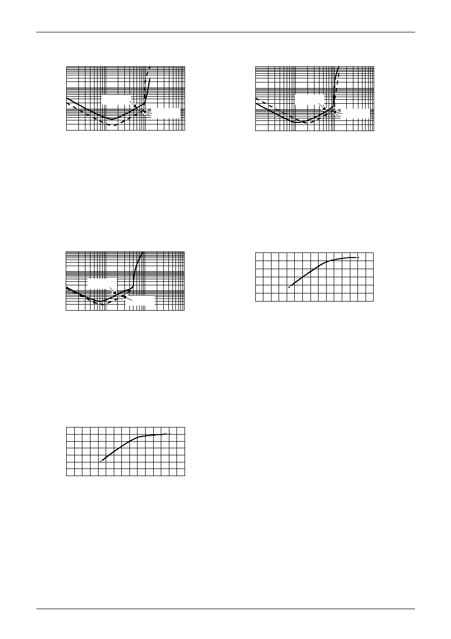
Characteristics
*
1 Resistor Tolerance ±1%
*
2 Capacitor Tolerance ±5%
*
3 The mute signal which switches off the power supply of a power amplifier that is connected with MM1454
appears in the 4 terminal. (NOTE 7)
*
4 The pop noise which occurs in a moment of the power supply switching on is reduced by connecting the
capacitor (10uF) between 2PIN and GND. But if the reduced pop noise cause trouble for your application, we
recommend muting the pop noise by the power amplifier that is connected with MM1454.
*
5 SW1: A QSurround Mode
SW2: B Bypass Mode
1. L
IN
-R
OUT
(R
IN
-L
OUT
) Frequency (Q Surround)
15.0
14.0
13.0
12.0
11.0
10.0
9.0
8.0
7.0
6.0
5.0
4.0
3.0
2.0
1.0
0.
100.0
10.0
1.0k
10.0k
100.0k
Frequency (Hz)
Voltage gain (dB)
2. L
IN
-R
OUT
(R
IN
-R
OUT
) Frequency (Q Surround)
Frequency (Hz)
10.0
8.0
6.0
4.0
2.0
0.
-2.0
-4.0
-6.0
-8.0
-10.0
100.0
10.0
1.0k
10.0k
100.0k
Voltage gain (dB)

MITSUMI
Q Surround Processor MM1454
3. THD of output signal - Input voltage (L
IN
) (QSrround)
Input Voltage (Vrms)
0.01
0.1
1
10
10
1
0.1
0.01
THD
( %
)
L
IN
-R
OUT
L
IN
-L
OUT
f=1kHz, R
IN
=0Vrms
4. THD of output signal - Input voltage (R
IN
) (QSrround)
Input Voltage (Vrms)
0.01
0.1
1
10
10
f=1kHz, R
IN
=0Vrms
1
0.1
0.01
THD
( %
)
R
IN
-L
OUT
R
IN
-R
OUT
5. THD of output signal - Input voltage (QSrround)
f=1kHz, The signals that are inputted in L
IN
and
R
IN
are out out of phase and same amplitude.
Input Voltage (Vrms)
0.01
0.01
0.1
1
10
0.1
1
10
THD
( %
)
L
OUT
R
OUT
6. Input voltage (1) - Power supply voltage (QSrround)
Power supply voltage V
CC
(V)
0
5
10
15
0
0.2
0.4
0.6
0.8
1
1.2
Input Voltage
( 1
) V
IN
1(
Vrms
)
7. Input voltage (2) - Power supply voltage (QSrround)
Power supply voltage V
CC
(V)
0
5
10
15
0
0.1
0.2
0.3
0.4
0.5
0.6
0.7
Input Voltage
( 2
)V
IN
2 (
Vrms
)
See Electrical Characteristics Note 1
See Electrical Characteristics Note 2


