MITSUMI
Op Amplifier 2 Circuit and Shunt Regulator (2.5V) MM1462BN, MM1462XN
Op Amplifier 2 Circuit and Shunt Regulator (2.5V)
Monolithic IC MM1462BN, MM1462XN
Outline
MM1462BN incorporates a 2-circuit op amp + shunt regulator (1.25V), and MM1462XN incorporates a 2-
circuit op amp + shunt regulator (2.5V).
Supports voltage control and sensors for adapters, etc.
Features
1. Input bias current
30nA typ.
2. Power supply voltage removal
65dB min. (B amp)
3. Current consumption
2.4mA typ. (MM1462BN)
1.2mA typ. (MM1462XN)
4. Reference voltage
1.25V typ. (MM1462BN)
2.50V typ. (MM1462XN)
5. Output inversion voltage fluctuation
3mV typ. (MM1462BN-A amp)
(V
CC
=2.5~5V)
0.5mV typ. (MM1462BN-B amp)
Package
SOT-25A
SOT-25B
Applications
1. Charger
2. Switching power supply
3. AC adapter
1
3
5
2
4
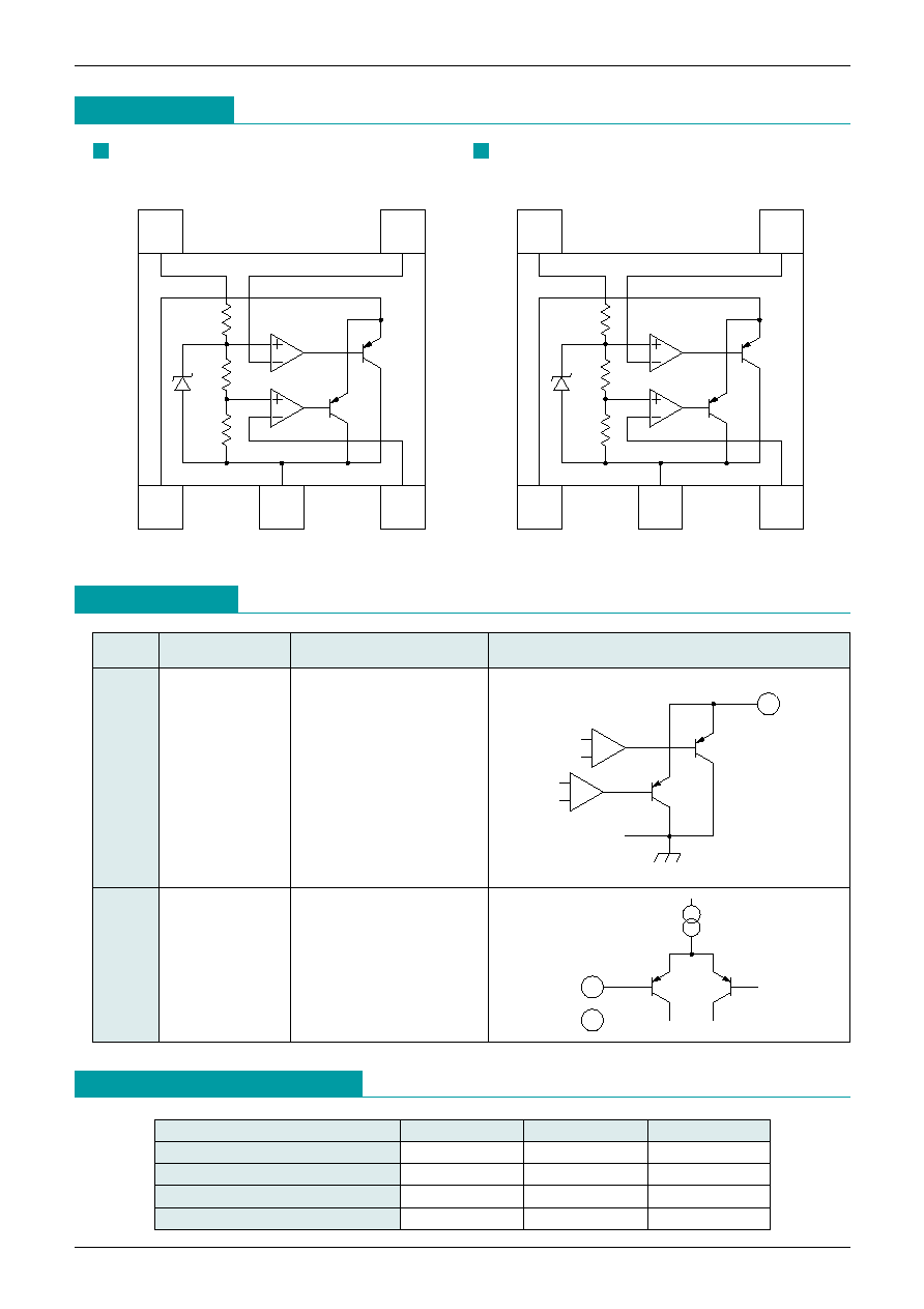
SOT-25A, SOT-25B
(TOP VIEW)
1
OUT
2
GND
3
B
IN
4
A
IN
5
V
CC
Pin Assignment

MITSUMI
Op Amplifier 2 Circuit and Shunt Regulator (2.5V) MM1462BN, MM1462XN
Block Diagram
IN
B
GND
OUT
3
1
2
3080
4000
46920
4
5
IN
CC
A
V
IN
B
GND
OUT
3
1
2
3097
2000
22057
4
5
IN
CC
A
V
Pin Description
Pin No.
Pin name
Function
Internal equivalent circuit diagram
1
4
3
1
OUT
Output pin
3
B
IN
Input pin
4
A
IN
MM1462XN
MM1462BN
Absolute Maximum Ratings
(Ta=25�C)
Item
Symbol
Ratings
Units
Strage temperature
T
STG
-40~+125
�C
Operating temperature
T
OPR
-25~+85
�C
Supply voltage
V
CC
max
-0.3~+20
V
Allowable loss
Pd
250
mW

MITSUMI
Op Amplifier 2 Circuit and Shunt Regulator (2.5V) MM1462BN, MM1462XN
Recommended Operating Conditions
Item
Symbol
Ratings
Units
Operating temperature
T
OPR
-20~+70
�C
Operating voltage
V
OPR
+2.5~+20
�C
Item
Symbol
Ratings
Units
Operating temperature
T
OPR
-25~+85
�C
Operating voltage
V
OPR
+4~+20
�C
Electrical Characteristics
(Except where noted therwise, Ta=25�C, V
CC
=5V)
Item
Symbol
Measurement conditions
Min. Typ. Max. Units
Current consumption
I
CC
A
IN
=0V, B
IN
=0V, RL=
2.4
3.4
mA
A amplifier
Output inverting voltage (A)
V
A
B
IN
=0V, RL=4.3k, V
CC
=3~5V
1.225 1.25 1.275
V
Input bias current (A)
I
B
B
IN
=0V, RL=4.3k
30
150
nA
PSRR (A)
PSRR
B
IN
=0V, RL=4.3k
50
dB
Output sink current (A)
I
SI
A
IN
=1.35V, B
IN
=0V, V
OUT
=1.5V
5
mA
Output inverting voltage (A)
V
A
B
IN
=0V, RL=4.3k, V
CC
=2.5~5V
3
mV
deviation
Output inverting voltage (A)
�100
ppm/�C
temperature coefficient
B amplifier
Output inverting voltage (B)
V
B
A
IN
=0V, RL=4.3k, V
CC
=3~5V
151
154
157
mV
Input bias current (B)
I
B
A
IN
=0V, RL=4.3k, V
CC
=3~5V
30
150
nA
PSRR (B)
PSRR
A
IN
=0V, RL=4.3k
65
dB
Output sink current (B)
I
SI
A
IN
=0V, B
IN
=0.17V, V
OUT
=1.5V
5
mA
Output inverting voltage (B)
V
B
A
IN
=0V, RL=4.3k, V
CC
=2.5~5V
0.5
mV
deviation
Output inverting voltage (B)
�100
ppm/�C
temperature coefficient
Item
Symbol
Measurement conditions
Min. Typ. Max. Units
Current consumption
I
CC
A
IN
=0V, B
IN
=0V, RL=
1.2
1.7
mA
A amplifier
Output inverting voltage (A)
V
A
B
IN
=0V, RL=4.3k
2.45
2.50
2.55
V
Input bias current (A)
I
B
B
IN
=0V, RL=4.3k
30
150
nA
PSRR (A)
PSRR (A)
B
IN
=0V, RL=4.3k
62
dB
Output sink current (A)
I
SI
A
IN
=2.7V, B
IN
=0V, V
OUT
=1.5V
5
mA
B amplifier
Output inverting voltage (B)
V
B
A
IN
=0V, RL=4.3k
151
154
157
mV
Input bias current (B)
I
B
A
IN
=0V, RL=4.3k
30
150
nA
PSRR (B)
PSRR (B)
A
IN
=0V, RL=4.3k
65
dB
Output sink current (B)
I
SI
A
IN
=0V, B
IN
=0.17V, V
OUT
=1.5V
5
mA
MM1462BN
MM1462XN
MM1462BN
MM1462XN

MITSUMI
Op Amplifier 2 Circuit and Shunt Regulator (2.5V) MM1462BN, MM1462XN
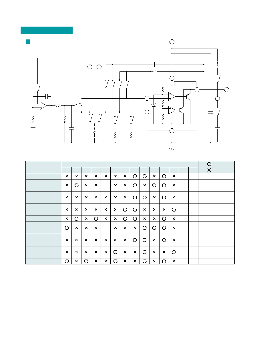
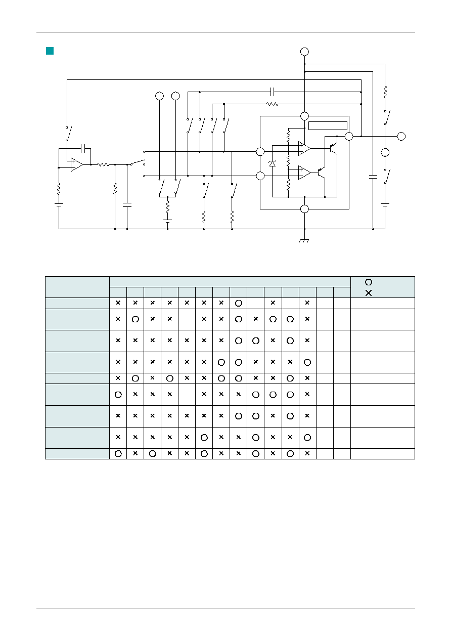
Measuring Circuit
OFF
22057
3097
2000
5
4
3
1
2
MM1462BNRE
SW1
SW2
SW3
SW4
GND
OUT
IN
B
IN
A
CC
V
SW6
SW7
TPB TPA
SW8
SW9
SW10
SW5
B
IN
A
IN
0.22
�
F
100k
0.22
�
F
1.5k
3.9k
1.5V
680k
A
1.5k
SW12
SW11
RL
47
�
F
V
IN
1k
1M
1M
0.1
�
F
CC
V
Item
Switch Status
: ON
SW1 SW2 SW3 SW4 SW5 SW6 SW7 SW8 SW9 SW10 SW11 SW12 RL (
) V
IN
(V)
: OFF
Current consunption
4.3k
Output inverting
A
IN
4.3k
Mesure TPA
voltage (A)
voltage
Input bias
4.3k
Mesure TPA
current (A)
voltage
Output sink
1.35
Mesure output
current (A)
sink current
PSRR (A)
4.3k V
A
*
1
Output inverting
B
IN
4.3k
Mesure TPB
voltage (B)
voltage
Input bias
4.3k
Mesure TPB
current (B)
voltage
Output sink
0.17
Mesure output
current (B)
sink current
PSRR (B)
4.3k
*
3
*
2
(Except where noted therwise, Ta=25�C, V
CC
=5.0V)
*
1
V
OUT
1 is defined by the voltage when V
CC
=4V. V
OUT
2 is defined by the voltage when V
CC
=25V.
PSRR (A) is shown in the eqation below.
*
2
V
OUT
1 is defined by the voltage when V
CC
=4V. V
OUT
2 is defined by the voltage when V
CC
=25V.
PSRR (B) is shown in the eqation below.
PSRR=40+20log | (25V-4V) / (V
OUT
1-V
OUT
2) |
*
3
VB-20mV
MM1462BN

MITSUMI
Op Amplifier 2 Circuit and Shunt Regulator (2.5V) MM1462BN, MM1462XN
OFF
46920
3080
4000
5
4
3
1
2
MM1462XNRE
SW1
SW2
SW3
SW4
GND
OUT
IN
B
IN
A
CC
V
SW6
SW7
TPB TPA
SW8
SW9
SW10
SW5
B
IN
A
IN
0.22
�
F
100k
0.22
�
F
1.5k
3.9k
1.5V
680k
A
1.5k
SW12
SW11
RL
47
�
F
V
IN
1k
1M
1M
0.1
�
F
CC
V
Item
Switch Status
: ON
SW1 SW2 SW3 SW4 SW5 SW6 SW7 SW8 SW9 SW10 SW11 SW12 RL (
) V
IN
(V)
: OFF
Current consunption
4.3k
Output inverting
A
IN
4.3k
Mesure TPA
voltage (A)
voltage
Input bias
4.3k
Mesure TPA
current (A)
voltage
Output sink
2.7V
Mesure output
current (A)
sink current
PSRR (A)
4.3k VA
*
1
Output inverting
B
IN
4.3k
Mesure TPB
voltage (B)
voltage
Input bias
4.3k
Mesure TPB
current (B)
voltage
Output sink
0.17
Mesure output
current (B)
sink current
PSRR (B)
4.3k
*
3
*
2
(Except where noted therwise, Ta=25�C, V
CC
=5.0V)
*
1
V
OUT
1 is defined by the voltage when V
CC
=4V. V
OUT
2 is defined by the voltage when V
CC
=25V.
PSRR (A) is shown in the eqation below.
*
2
V
OUT
1 is defined by the voltage when V
CC
=4V. V
OUT
2 is defined by the voltage when V
CC
=25V.
PSRR (B) is shown in the eqation below
PSRR=40+20log | (25V-4V) / (V
OUT
1-V
OUT
2) |
*
3
VB-20mV
MM1462XN

MITSUMI
Op Amplifier 2 Circuit and Shunt Regulator (2.5V) MM1462BN, MM1462XN
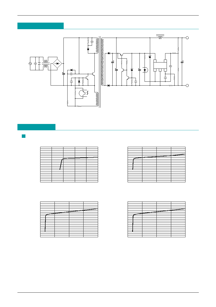
Application Circuit
MM1462XN
3
5
4
2
1
0.1
�
F
8.3
�
/250V
0.033
�
F
0.022
�
F
8.2k
100
100
2.7k
56k
0.001
�
/1kV
800
�
/8V
/16V
100
�
47k
1M
390
100
0.1
�
F
0.22
390
1.5k
0.1
�
F
1k
/16V
100
�
68
�
H
1.5k
B+
GND
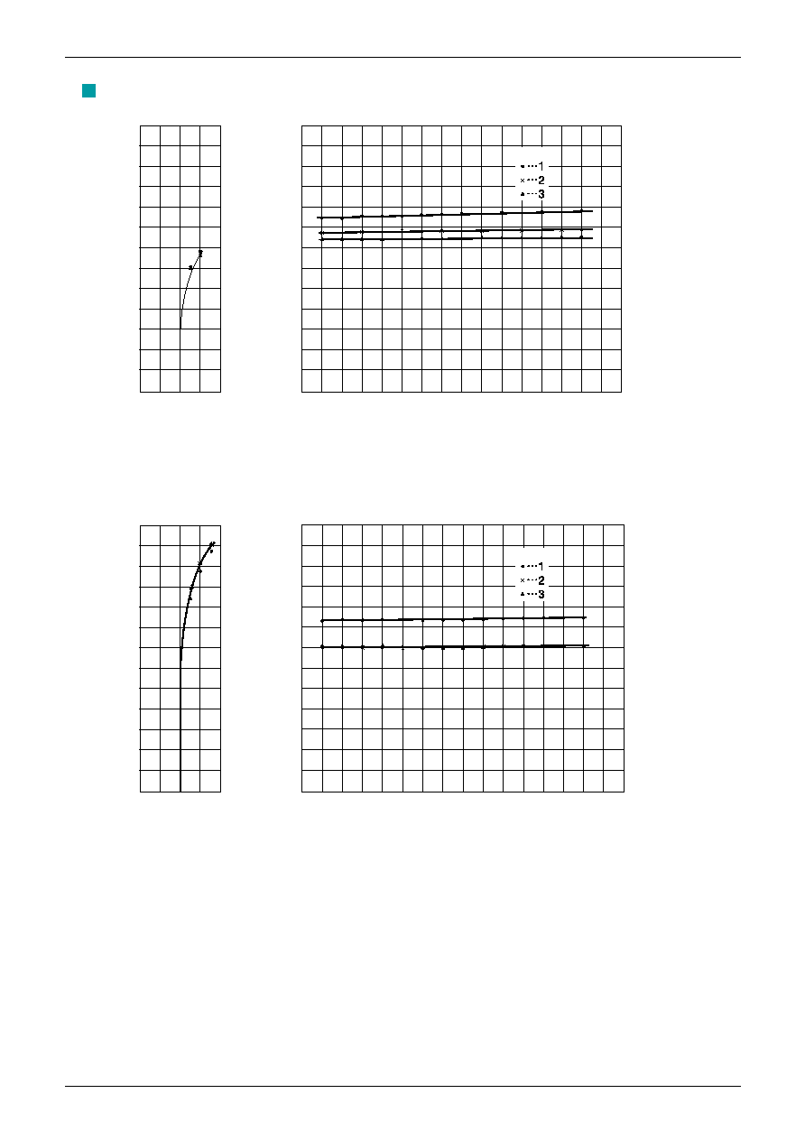
Characteristics
(3.0V product except where noted therwise, Ta=25�C, V
IN
=5V, V
CONT
=5V, C
IN
=1�F, C
O
=2.2�)
1.10
4
5
2
3
1
0
V
CC
(V)
1.30
1.25
1.20
1.15
Output Inverting
Voltage A (V)
1.10
20
10
15
5
0
1.30
1.25
1.20
1.15
V
CC
(V)
Output Inverting
Voltage A (V)
0.140
4
2
3
1
0
0.160
0.155
0.150
0.145
V
CC
(V)
Output Inverting
Voltage B (V)
0.140
4
2
3
1
0
0.160
0.155
0.150
0.145
V
CC
(V)
Output Inverting
Voltage B (V)
Note: these are typical characteristics
MM1462BN

MITSUMI
Op Amplifier 2 Circuit and Shunt Regulator (2.5V) MM1462BN, MM1462XN
14
30
28
26
24
22
20
18
16
12
10
6
4
0.149
0.150
0.151
0.152
0.153
0.154
0.155
0.156
0.157
0.158
0.159
0.02
0
0.04
0.06
0.08
0.10
0.12
0.14
0.16
8
3
0
1
2
V
CC
(V)
V
CC
(V)
Sample No.
Output Inverting Voltage B (V)
Output Inverting Voltage B (V)
Sample No.
14
30
28
26
24
22
20
18
16
12
10
6
4
2.45
2.44
2.46
2.47
2.48
2.49
2.50
2.51
2.52
2.53
2.54
2.55
1.8
2.0
2.2
2.4
2.6
0.02
0
0.04
0.06
0.08
0.10
0.12
0.14
0.16
8
3
0
1
2
V
CC
(V)
V
CC
(V)
Output Inverting Voltage B (V)
Output Inverting Voltage B (V)
Note: these are typical characteristics
MM1462XN

