 | –≠–Ľ–Ķ–ļ—ā—Ä–ĺ–Ĺ–Ĺ—č–Ļ –ļ–ĺ–ľ–Ņ–ĺ–Ĺ–Ķ–Ĺ—ā: MM1516 | –°–ļ–į—á–į—ā—Ć:  PDF PDF  ZIP ZIP |

MITSUMI
Composite regulator with ON/OFF MM1516
Composite regulator with ON/OFF
Monolithic IC MM1516
Outline
This IC was developed as a compound power supply and is composed of 3 positive voltage regulator
circuits. Regulator output voltage is fixed, and A ranks are set at 2.5V typ. 2.8V typ. and 3.0V typ. Switch
pins are provided to control each output. This IC is ideal for use in cellular telephones and the like.
Features
1. Input/output voltage difference V
O
1: 0.25V typ.
V
O
2: 0.28V typ.
V
O
3: 0.30V typ.
2. Output noise voltage
V
O
1: 60ĶVrms typ.
V
O
2: 60ĶVrms typ.
V
O
3: 60ĶVrms typ.
3. Output voltage precision
V
O
1, V
O
2, V
O
3: Ī3%
4. No-load input current
V
O
1: 250ĶA typ.
V
O
2, V
O
3: 500ĶA
5. Input voltage
12V max.
6. Maximum output current
I
O
1: 100mA max.
I
O
2: 100mA max.
I
O
3: 150mA max.
7. Output ON/OFF control
High: ON, Low: OFF
Package
VSOP-8B
Applications
1. Cellular telephones, PHS
2. Video cameras
3. Portable communications equipment
4. Battery-powered portable equipment
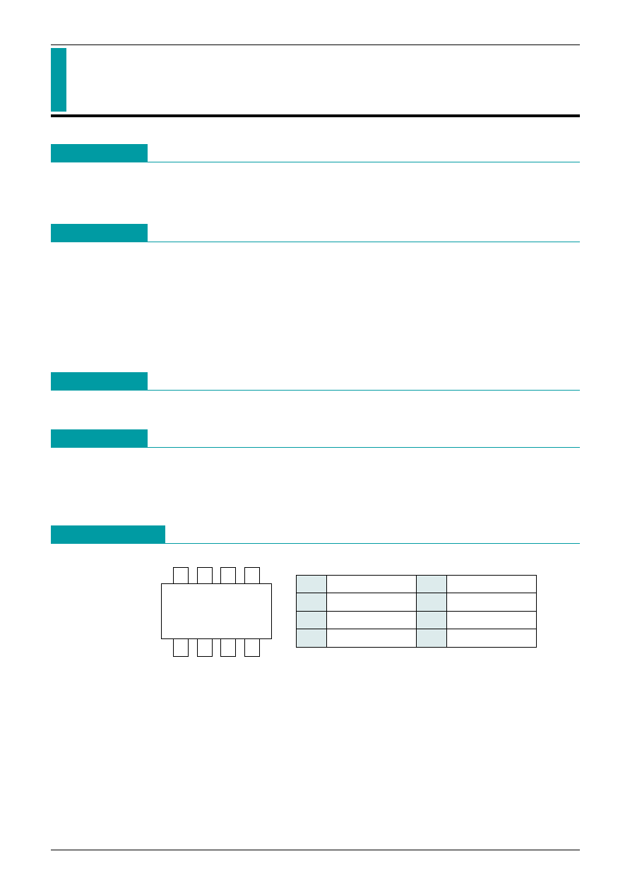
Pin Assignment
1
4
3
2
8
5
6
7
VSOP-8B
(TOP VIEW)
MITSUMI
1
PS1
5
Vo3
2
PS2/3
6
Vo2
3
NC
7
Vo1
4
V
IN
8
GND

MITSUMI
Composite regulator with ON/OFF MM1516
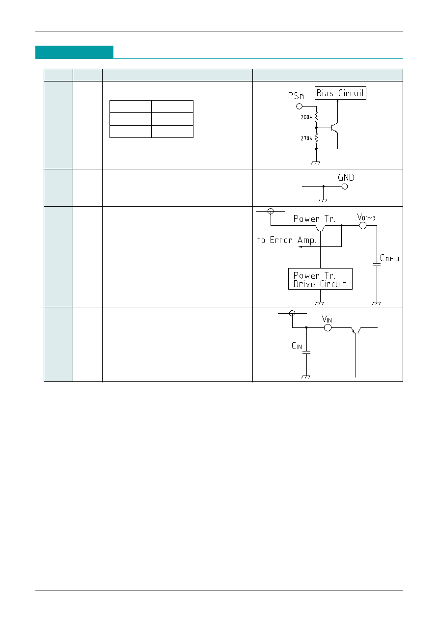
Pin Description
MITSUMI
Pin No. Pin name
Functions
Internal equivalent circuit
1
PSn
ON/OFF-Control Pin
2
Connect Cont-Terminal With V
IN,
When It Is Not Used.
8
GND
GND Pin
5
Vo1~3
Regulator Output Pin
6
7
4
V
IN
Voltage-supply Pin
V
SPn
Output
L
OFF
H
ON

MITSUMI
Composite regulator with ON/OFF MM1516
Equivalent Circuit Diagram

MITSUMI
Composite regulator with ON/OFF MM1516
MITSUMI
Electrical Characteristics
(Ta=25įC, V
IN
=, C
IN
=2.2Ķ, C
VO
(n) =2.2ĶF Funless otherwise spec. )
Item
Symbol
Measurement conditions
Min. Typ. Max. Unit
Supply Current(off)
I
IN
V
PS1
=V
PS2/3
=0V
0
3
ĶA
Supply Current1~3
No load
(1 circuit's worth is
I
IN
1~3
I
IN
1
V
PS1
=3V, V
PS2/3
=0V
250
370
ĶA
the same as 3 circuits)
I
IN
2/3
V
PS2
=3V, V
PS1/3
=0V
500
740
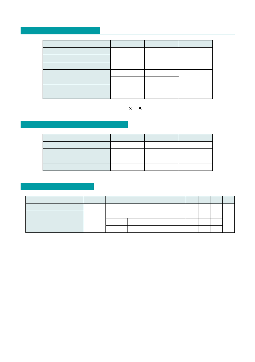
Absolute Maximum Ratings
Item
Symbol
Ratings
Unit
Operating Temperature
T
OPR
-20~+75
įC
Storage Temperature
T
STG
-40~+125
įC
Supply Voltage
V
IN
-0.3~+12
V
Output Current
I
O
(1,2)
100
mA
I
O
(3)
150
Power Dissipation
Pd
300 (
*
1)
500 (
*
2)
mW
Recommended Operating Conditions
Item
Symbol
Ratings
Unit
Operating Temperature
T
OP
-20~75
įC
Regulator Output Current
I
O
(1,2)
0~70
mA
I
O
(3)
0~100
Operating Voltage
V
OP
1.8~8
V
(
*
1) Alone measurement
(
*
2)When mounted on glass epoxy board (40 40 1.6mm)

MITSUMI
Composite regulator with ON/OFF MM1516
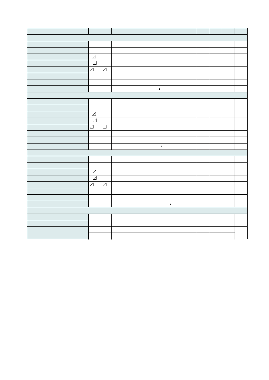
Item
Symbol
Measurement conditions
Min. Typ. Max. Unit
Vo1
Output Voltage
Vo1
I
01
=30mA
2.42
2.50
2.58
V
Input-Output Differetial Voltage
Vdmin.1
V
IN
=2.3V, I
01
=30mA
0.1
0.25
V
Load Regulation
VLo1
I
01
=0~70mA
30
60
mV
Line Regulation
VLi1
V
IN
=4.0~8.0V, I
01
=30mA
10
25
mV
Vo Temperature Coefficient (
*
)
Vo1/ T
Tj=-20~75įC, I
01
=30mA
Ī100
ppm/įC
Ripple Rejection (
*
)
RR1
f=120Hz, Vripple=1V
P-P
I
01
=30mA
50
60
dB
Output Noise Voltage (
*
)
Vn1
f=10Hz~10kHz, I
01
=30mA
60
90
ĶVrms
Output Delay Time (
*
)
TdH1
I
01
=30mA, V
PS1
=0 4V,V
PS2/3
=0V
0.04
0.15
ms
Vo2
Output Voltage
Vo2
I
02
=30mA
2.72
2.80
2.88
V
Input-Output Differetial Voltage
Vdmin.2
V
IN
=2.6V, I
02
=30mA
0.1
0.25
V
Load Regulation
VLo2
I
02
=0~70mA
30
60
mV
Line Regulation
VLi2
V
IN
=4.0~8.0V, I
02
=30mA
10
25
mV
Vo Temperature Coefficient (
*
)
Vo2/ T
Tj=-20~75įC, I
02
=30mA
Ī100
ppm/įC
Ripple Rejection (
*
)
RR2
f=120Hz, Vripple=1V
P-P
I
02
=30mA
50
60
dB
Output Noise Voltage (
*
)
Vn2
f=10Hz~10kHz, I
02
=30mA
60
90
ĶVrms
Output Delay Time (
*
)
TdH2
I
02
=30mA, V
PS2/3
=0 4V V
PS1
=0V
0.04
0.15
ms
Vo3
Output Voltage
Vo3
I
03
=80mA
2.92
3.00
3.08
V
Input-Output Differetial Voltage
Vdmin.3
V
IN
=2.8V, I
03
=80mA
0.15
0.30
V
Load Regulation
VLo3
I
03
=0~100mA
30
60
mV
Line Regulation
VLi3
V
IN
=4.0~8.0V, I
03
=30mA
10
25
mV
Vo Temperature Coefficient (
*
)
Vo3/ T
Tj=-20~75įC, I
03
=30mA
Ī100
ppm/įC
Ripple Rejection (
*
)
RR3
f=120Hz Vripple=1V
P-P
I
03
=30mA
50
60
dB
Output Noise Voltage (
*
)
Vn3
f=10Hz~10kHz, I
03
=30mA
60
90
ĶVrms
Output Delay Time (
*
)
TdH3
I
03
=30mA, V
PS2/3
=0 4V
0.04
0.15
ms
PS output control pin
Low Threshold Voltage
V
OFF
0.4
V
High Threshold Voltage
V
ON
1.6
V
PS(n) Terminal Current
I
PS1
V
PS1
=1.6V
8
ĶA
I
PS2/3
V
PS2/3
=1.6V
16
Note:This spec is guaranteed by design.

MITSUMI
Composite regulator with ON/OFF MM1516
MITSUMI
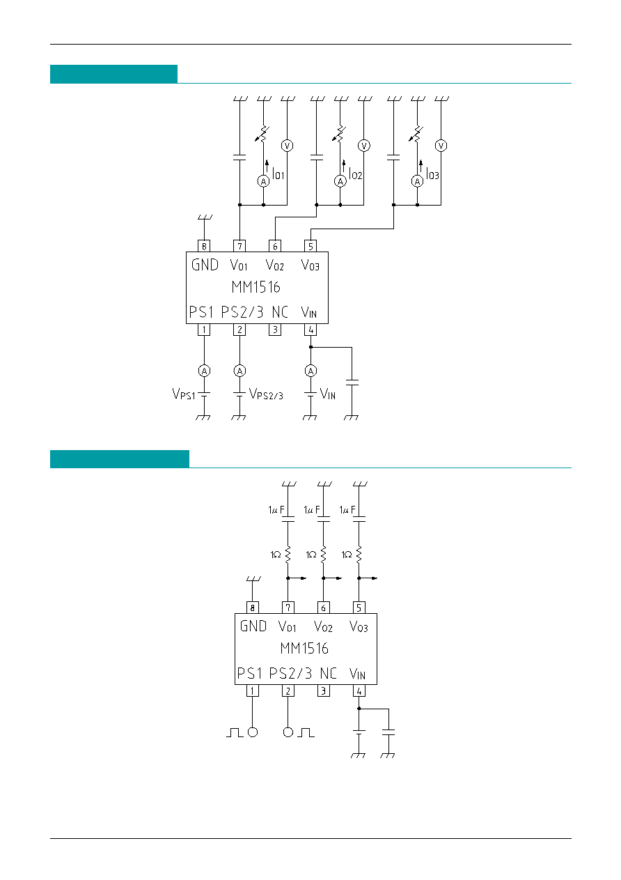
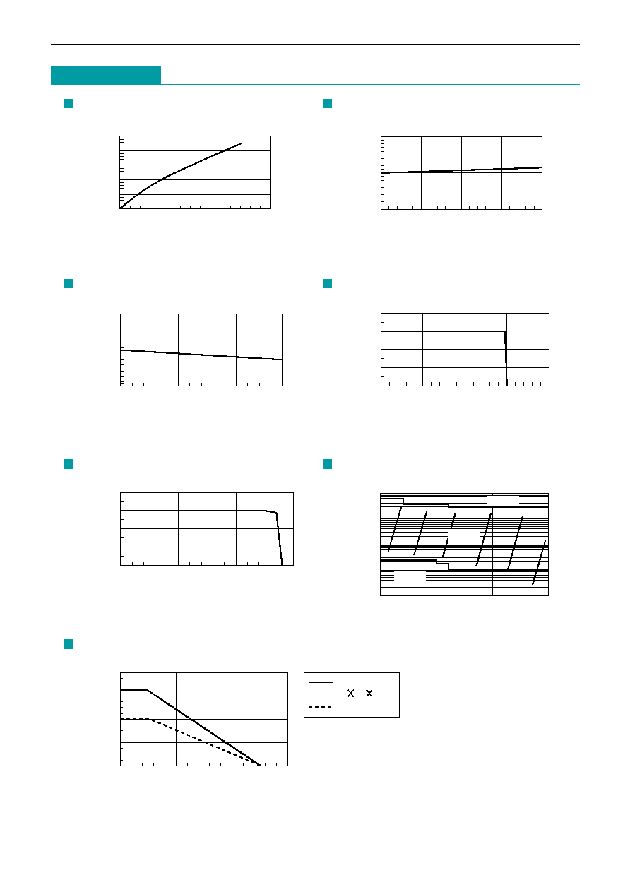
Application Circuits
Note:This regulator is not internally compensated and thus requires an external output-capacitor(Cvo) for
stability.
Measuring Circuit

MITSUMI
Composite regulator with ON/OFF MM1516
MITSUMI
Characteristics
0
150
100
50
0
Output Current (mA)
200
150
100
50
250
Input-Output (mV)
Vin (V)
-20
12
10
6
8
4
10
0
-10
20
Line Regulation (mV)
Input-Output Differetial Voltage
Line Regulation
Output Current (mA)
-60
150
100
50
0
20
0
40
-20
-40
60
Load Regulation
(mV)
Temperature (
į
C)
0
200
150
50
100
0
3
2
1
4
Output Voltage (V)
Load Regulation
Thermal Shutdown
Output Current (mA)
0
300
100
200
0
3
2
1
4
Output Voltage (V)
Current Limit
Load Current (mA)
0.01
150
100
50
0
10
1
0.1
100
ESR (
)
Instable
Stable
Instable
ESR Stable
Temperature (
į
C)
0
150
50
100
0
600
400
200
800
Alone
Allowable loss (mW)
On Board
40 40 1.6mm
Allowable loss
Note: Reference data
