 | –≠–ª–µ–∫—Ç—Ä–æ–Ω–Ω—ã–π –∫–æ–º–ø–æ–Ω–µ–Ω—Ç: MM1532 | –°–∫–∞—á–∞—Ç—å:  PDF PDF  ZIP ZIP |

MITSUMI
Lithium Ion Battery Charging Control MM1532
Lithium Ion Battery Charging Control
Monolithic IC MM1532
Outline
This IC is a lithium ion battery charging controller, with protection circuits such as constant-current, constant-
voltage charging and pre-charge, battery temperature detection function and others all on one chip.
The timer function on charging IC MM1475 has been omitted to achieve a smaller package, changed SW
function from MM1485.
Features
1. Output voltage (Ta = 0 ~ +50∞C)
4.200±30mV
2. Consumption current 1
1.5mA typ.
Pre-charge function
Adaptor (primary side) abnormality detection function
3. Battery temperature detection function
Package
TSOP-16A
Applications
1. Lithium ion battery charging control
MITSUMI
Absolute Maximum Ratings
(Ta=25∞C)
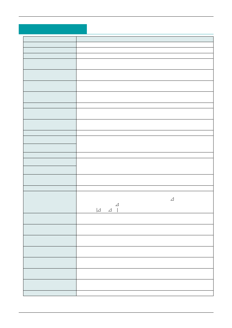
Item
Symbol
Ratings
Unit
Storage temperature
T
STG
-40~+125
∞C
Operating temperature
T
OPR
-20~+70
∞C
Power supply voltage
V
CCMAX
-0.3~+15
V
Allowable loss
P
D
250
mW
SW2 Input voltage
V
SW2
-0.3~V
CC
+0.3
V

MITSUMI
Lithium Ion Battery Charging Control MM1532
MITSUMI
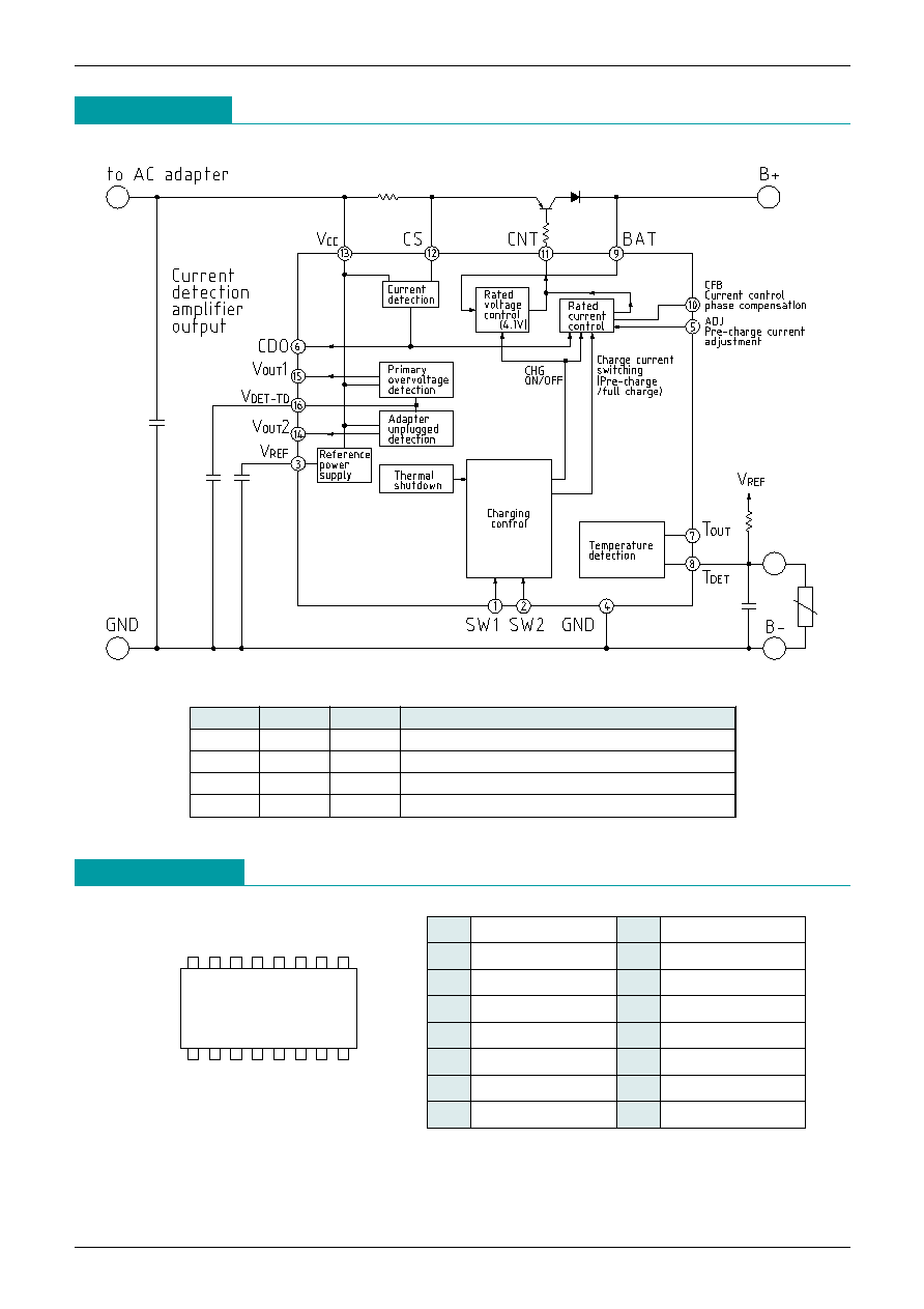
Block Diagram
SW1
SW2
Charge
Current Limit
L
H
ON
Controlled by the adaptor (current limit 1:450mV)
H
H
ON
Controlled by the adaptor (current limit 1:450mV)
L
L
OFF
H
L
ON
Controlled by the IC (current limit 2:25mV)
SW1 and SW2 Specifications
Pin Assignment
TSOP-16A
1
3
7
6
2
4 5
8
16
13
11
15 14
12
9
10
1
SW1
9
BAT
2
SW2
10
CFB
3
V
REF
11
CNT
4
GND
12
CS
5
ADJ
13
V
CC
6
CDO
14
V
OUT2
7
T
OUT
15
V
OUT1
8
T
DET
16
V
DET
-
TD

MITSUMI
Lithium Ion Battery Charging Control MM1532
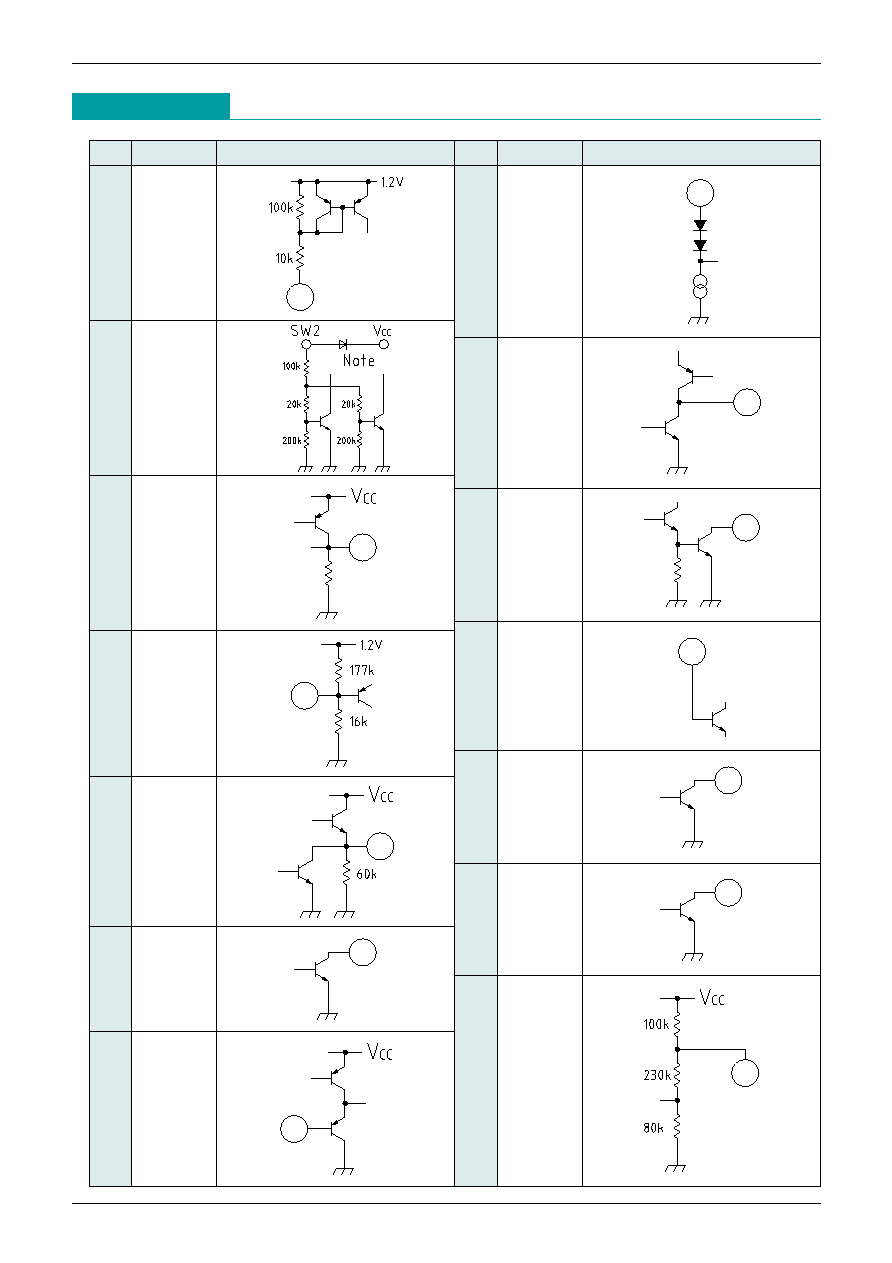
Pin Description
Pin No.
Pin Name
I/O
Function
1
SW1
Input
Charging control switching pin.
Switches charging ON/OFF and charging current by combinations of SW1
and SW2 L and H.
2
SW2
Input
3
V
REF
Output
Pre-charge current adjustment pin.
Pin voltage is set at 100mV typ. Pre-charge current can be adjusted by
adjusting the pin voltage with an external resistor, etc.
Pre-charge current is controlled by comparing the ADJ pin voltage and voltage
drop value of 12dB between V
CC
-CS.
Reference power supply output pin.
Outputs 1.2V typ. reference voltage.
5
ADJ
Input
Current detection output pin.
Outputs current difference value of 18dB between V
CC
-CS.
GROUND pin.
6
C
DO
Output
4
GND
Input
Temperature detection output pin.
Normal temperature: Output Tr OFF
High temperature detection: Output Tr ON
7
T
OUT
Output
8
T
DET
Input
Temperature detection input pin.
Use external resistor and thermistor to apply resistance-divided potential from
reference voltage.
9
BAT
Input
Battery voltage input pin.
Detects battery voltage and controls charging.
10
CFB
Input
Constant-current control phase compensation pin.
Connect an external capacitor (around 100pF) between CFB and CNT to
perform phase compensation for improved oscillation.
12
CS
Input
Current detection pin.
Current is detected by voltage drop at external resistor between V
CC
-CS and
charging current is controlled.
11
CNT
Output
Charging control output pin.
Controls external PNP-Tr base and performs constant-current, constant-
voltage charging.
13
V
CC
Input
Power supply input pin.
14
V
OUT2
Output
Adaptor unplugged detection output pin.
V
CC
low voltage input: Output Tr OFF
V
CC
recommended operating voltage: Output Tr ON
15
V
OUT1
Output
Overvoltage detection output pin.
V
CC
overvoltage input: Output Tr OFF
V
CC
recommended operating voltage: Output Tr ON
16
V
DET
-TD
Input
Overvoltage detection delay time setting pin.
Delay time can be set by connecting an external capacitor.

MITSUMI
Lithium Ion Battery Charging Control MM1532
Pin Description
The following valaeis typical
Pin No. Pin name
Internal equivalent circuit diagram
Pin No. Pin name
Internal equivalent circuit diagram
1
SW1
10
CFB
11
CNT
2
SW2
3
VREF
5
ADJ
6
CDO
7
TOUT
8
TDET
9
BAT
12
CS
14
VOUT2
15
VOUT1
16
VDET-TD

MITSUMI
Lithium Ion Battery Charging Control MM1532
Electrical Characteristics
(Except where otherwise indicated Ta=25∞C, V
CC
=5V)
Item
Symbol
Conditions
Measurement
Min. Typ. Max. Unit
pin
Consumption current 1
I
CC1
V
SW1
=1.2, V
SW2
=0V
13
1.5
2.3
mA
Consumption current 2
I
CC2
V
SW1
=0, V
SW2
=5V
13
3.5
5.3
mA
Reference voltage
V
REF
3
1.207
V
ADP detection voltage L
V
ADPL
V
CC
: H L
14
2.70
2.80
2.90
V
ADP detection voltage L
hysteresis voltage width
V
ADPLW
14
50
100
150
mV
ADP detection voltage H
V
ADPH
V
CC
: L H
15
5.8
6.0
6.2
V
ADP detection voltage H
hysteresis voltage width
V
ADPHW
15
50
100
150
mV
BAT pin leak current
I
BAT
9
1
µA
BAT pin output voltage
V
BAT
Ta=0~+50∞C
9
4.170 4.200 4.230
V
CNT pin output voltage
V
CNT
I
CNT
=20mA
11
0.5
V
SW1 pin input current
I
SW1
1
40
60
80
µA
SW1 pin input voltage H
V
SW1H
1
0.6
1.20
V
SW1 pin input voltage L
V
SW1L
1
0.25
V
SW2 pin input current
I
SW2
2
6
12
18
µA
SW2 pin input voltage H
V
SW2H
2
2
V
CC
V
SW2 pin input voltage L
V
SW2L
2
0.25
V
Current limit 1
V
L1
Quick charge
12,13
0.35
0.45
0.55
V
Current limit 2
V
L2
Pre-charge
12,13
20
25
30
mV
Current detection amp gain
G
I
6
17.5
18.0
18.5
dB
Current detection amp output
offset voltage
V
OFF
6
-4.5
0
4.5
mV
Current detection amp output
current outflow
I
CDO
6
0.5
1.0
mA
V
OUT1
pin output voltage
V
OUT1
I
OUT1
=0.12mA
15
0.2
0.4
V
V
OUT2
pin output voltage
V
OUT2
I
OUT2
=0.12mA
14
0.2
0.4
V
Battery temperature detection voltage
V
TDET
V
TDET
: H L
8
0.390 0.413 0.435
V
Battery temperature detection voltage
hysteresis voltage width
V
TDETW
8
30
60
90
mV
T
OUT
pin output voltage
V
TOUT
I
TOUT
=0.12mA
7
0.2
0.4
V
T
DET
input bias current
I
T
8
30
150
nA
*
Current limits 1 and 2 are prescribed by the amount of current detection resistor voltage drop.
*
Safety can not be guaranteed if this IC is damaged and control no longer is possible. Please protect with
something other than this IC.

MITSUMI
Lithium Ion Battery Charging Control MM1532
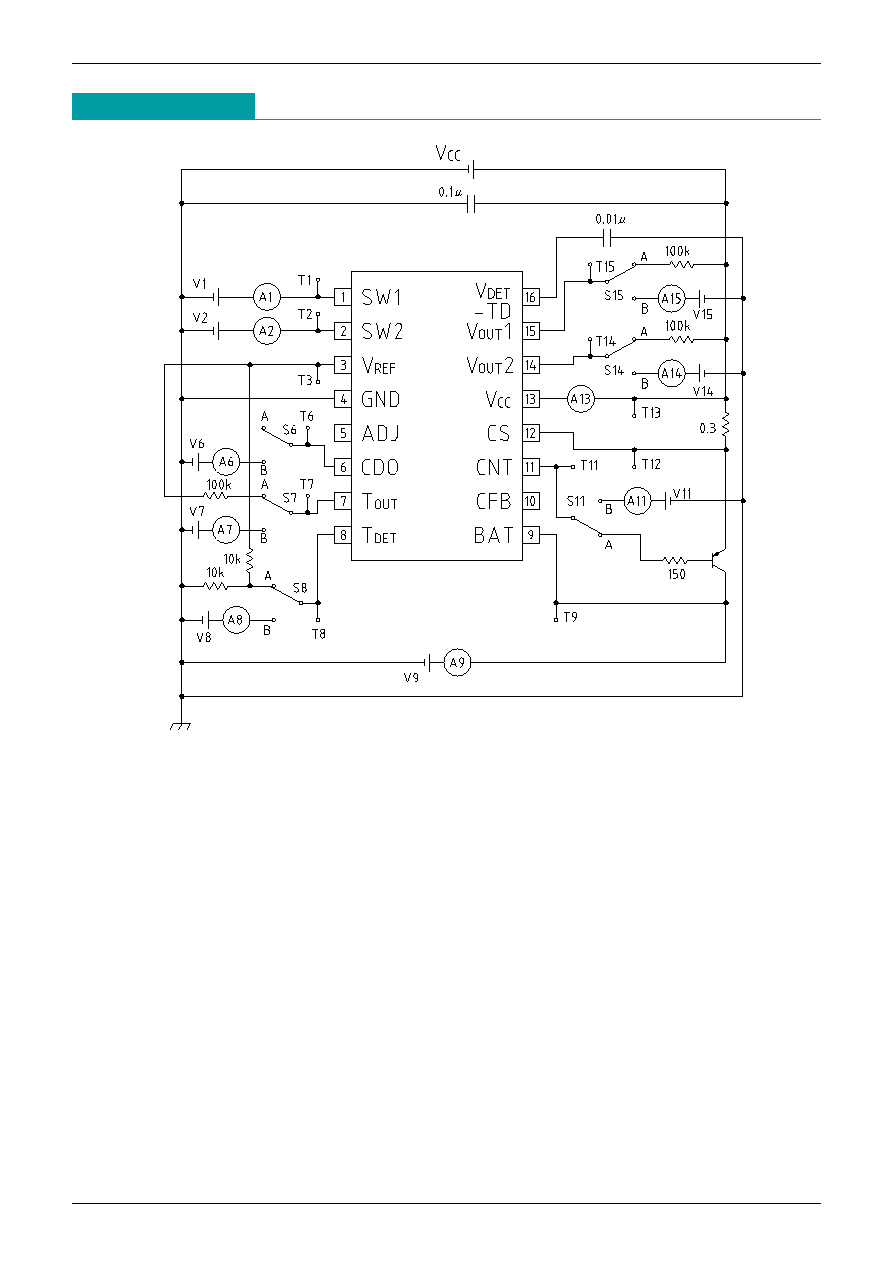
Measuring Circuit

MITSUMI
Lithium Ion Battery Charging Control MM1532
MITSUMI
Measurement Procedures
(Except where otherwise indicated Ta = 25∞C, V
CC
= 5V, V
CC
: current limit
0.5A, V1 = 0V, V2 = V
CC
, V9 = 4.27V, S6, 7, 8, 11, 14, 15: A)
Item
Measurement Procedure
Consumption current 1
Measure A13 current value I
CC1
at V1 =1.2V, V2 = 0V.
Consumption current 2
Measure A13 current value I
CC2
.
Reference voltage
Measure T3 potential V
REF
.
ADP detection voltage L
Gradually lower V
CC
from 5V. V
CC
potential is V
ADPL
when T14 potential goes
above V
CC
- 0.5V.
Gradually raise V
CC
from 2V. V
CC
potential is V
ADPL2
when T14 potential goes
under 0.5V. V
ADPLW
= V
ADPL2
- V
ADPL
ADP detection voltage H
Gradually raise V
CC
from 5V. V
CC
potential is V
ADPH
when T15 potential goes
above V
CC
- 0.5V.
Gradually lower V
CC
from 7V. V
CC
potential is V
ADPH2
when T15 potential goes
under 0.5V. V
ADPHW
= V
ADPH
- V
ADPH2
.
BAT pin leak current
V
CC
= 0V, V2=0V, S11: B, V11 = 0V. Measure A9 current value I
BAT
.
BAT pin output voltage
Gradually raise V9 from 3.5V. T9 potential is V
BAT
when the potential difference
between T13-T12 is 20mV or less.
CNT pin output voltage
V9 = 3.5V, S11: B. Gradually raise V11 from 0V. T11 potential is V
CNT
when A11
current value is 20mA.
SW1 pin input current
Measure A1 current value I
SW1
.
V9 = 3.5V, V2 = 0V. Raise V1 from 0V to 1.2V. Identify V
SW1
H or L; when A9 is
50mA or higher, charging ON at current limit 2, and when A9 is 1mA or lower,
charging is OFF.
SW2 pin input current
V1=0V, V2=2V. Measure A2 current value I
SW2
.
V9 = 3.5V, V1=0V. Raise V2 from 0V to V
CC
. Identify V
SW2
H or L; when A9 is
450mA or higher, charging ON at current limit 1, and when A9 is 1mA or lower,
charging is OFF.
Current limit 1
V1 = 0V, V2=V
CC
, V9=3.5V. Gradually raise V
CC
current limit value and measure
the potential difference between T13-T12, V
L1
.
Current limit 2
V1 = 1.2V, V2=0V, V9=2.5V. Potential difference between T13-T12 is V
L2
.
Current detection amp gain
V9 = 3.5V. The potential difference fluctuation between T13-T12 when V
CC
current limit value is changed from 100mA to 200mA is Va and the T6
potential fluctuation is Vb.
G
1
= 20log Vb/ Va
V9 = 4.0V. T6 potential is Vb2 when V
CC
current limit is 100mA.
V
OFF
= Vb2/8 - 30mV
V9 = 3.5V, V
CC
current limit value is 300mA, S6: B, V6 = 0V. Measure A6
current value.
V
OUT1
pin output voltage
S15: B. Gradually raise V15 from 0V. T15 potential is V
OUT1
when A15 current
value is 0.12mA.
V
OUT2
pin output voltage
S14: B. Gradually raise V14 from 0V. T14 potential is V
OUT2
when A14 current
value is 0.12mA.
S8: B. Gradually lower V8 from 0.6V. T8 potential is V
TDET
when T7 potential is
0.3V or under.
S8: B. Gradually raise V8 from 0V. T8 potential is V
TDET2
when T7 potential is
0.8V or higher. V
TDETW
= V
TDET2
- V
TDET
.
T
OUT
pin output voltage
S8: B, V8 = 0V, S7: B. Gradually raise V7 from 0V. T7 potential is V
TOUT
when
A7 current value is 0.12mA.
T
DET
input bias current
S8: B, V8 = 0V. Measure A8 potential value I
T
.
ADP detection voltage L
hysteresis voltage width
ADP detection voltage H
hysteresis voltage width
SW1 pin input voltage H
SW1 pin input voltage L
Current detection amp
output current outflow
Battery temperature detection
voltage hysteresis voltage width
Battery temperature detection
voltage hysteresis voltage width
Current detection amp
output offset voltage
SW2 pin input voltage H
SW2 pin input voltage L

MITSUMI
Lithium Ion Battery Charging Control MM1532
V
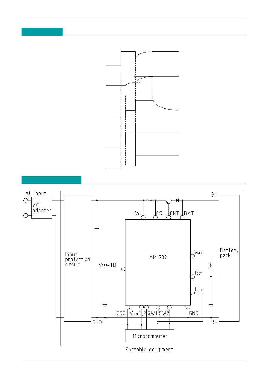
CC :
ON
Start
5V
4.20V
3V
2V
Full charge
Pre-
charge
H
L
L
H
OV
OA
Charging current
BAT pin voltage
SW1
SW2
V
CC
Timing Chart
Application Circuits

MITSUMI
Lithium Ion Battery Charging Control MM1532
Characteristics
0.3
0.35
0.4
0.45
0.5
0.55
-25
0
25
50
75
0.6
Ambient temperature (
∞
C)
Current Limit 1 (V)
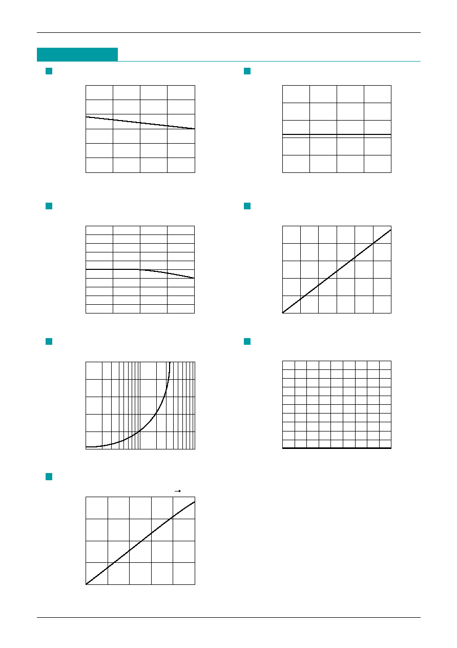
Current Limit 1 vs Ambient temperature
0
10
20
30
40
-25
0
25
50
75
50
Ambient temperature (
∞
C)
Current Limit 2 (mV)
Current Limit 2 vs Ambient temperature
4.15
-25
0
25
50
75
4.25
4.24
4.23
4.22
4.21
4.20
4.19
4.18
4.17
4.16
When VBAT=4.2V
Ambient temperature (
∞
C)
BAT Pin Output Voltage (V)
BAT Pin Output Voltage vs Ambient temperature
0
0.5
1
1.5
2
0
50
100
150
200
250
300
2.5
Ta=25
∞
C
Potential Difference between (CS+) and (CS-) (mV)
CDO Output Voltage (V)
Current Detection Input/Output
0
0.1
0.2
0.3
0.4
0
10
100
0.5
ICNT Current (mA)
VCNT Voltage (V)
Ta=25
∞
C
VCNT Voltage vs ICNT Current
0
0 0.5 1 1.5 2 2.5 3 3.5 4 4.5
0.1
0.09
0.08
0.07
0.06
0.05
0.04
0.03
0.02
0.01
Ta=25
∞
C
BAT Pin Voltage (V)
BAT Reverse Current (
µ
A)
BAT Pin Reverse Current vs BAT Pin Voltage
0
5
10
15
0
0.02
0.04
0.06
0.08
0.1
2
Ta = 25
∞
C, Vcc = 0 6.5V
Capacitance between (VDET-TD) and GND (
µ
F)
ADP Detection H Delay Time (ms)
ADP Detection H Delay Time
