 | –≠–ª–µ–∫—Ç—Ä–æ–Ω–Ω—ã–π –∫–æ–º–ø–æ–Ω–µ–Ω—Ç: MM1563D | –°–∫–∞—á–∞—Ç—å:  PDF PDF  ZIP ZIP |

MITSUMI
500mA Regulator MM156 F
500mA Regulator
Monolithic IC MM156 F
Outline
This IC is a small, stable power supply with output voltage precision of ±2% (when I
O
= 250mA), maximum
output current of 500mA, and I/O voltage difference of 0.3V typ. at 250mA.
Output noise reduction and output ON/OFF control pins are provided, making it ideal for portable equipment.
Features
1. No-load current consumption
1.9mA typ.
2. I/O voltage difference
0.3V typ. (I
O
=250mA)
3. Ripple rejection rate
64dB typ. (f=120Hz, V
RIPPLE
=1V
P-P
, I
O
=250mA)
4. Output current
500mA max.
5. Output noise voltage
75µVrms typ.
6. Output voltage rank
1.8 ~ 5.0V (0.1V steps)
7. Output ON/OFF control
High ON, Low OFF
Package
SOP-7B
Applications
1. Cordless telephone
2. Portable equipment, etc.
1
4
2
3
7
6
5
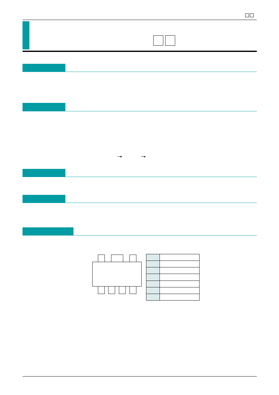
SOP-7B
(TOP VIEW)
1
V
O
2
NC
3
GND
4
Cn
5
CONT
6
Sub
7
V
IN
Pin Assignment

MITSUMI
500mA Regulator MM156 F
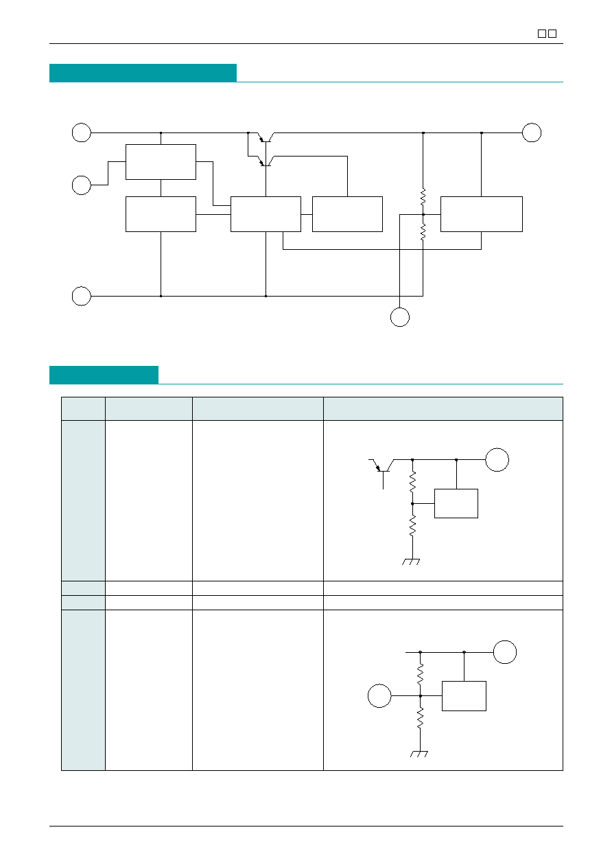
Equivalent Circuit Diagram
GND
V
IN
Thermal
shutdown
Bias
Cont
Driver
limitter
Current
Cn
Reference
O
V
Pin Description
Pin No.
Pin name
Function
Internal equivalent circuit diagram
Error
Amp.
OUT
V
Error
Amp.
OUT
V
C
n
1
V
OUT
Output pin
2
NC
No connection
3
GND
Ground
4
Cn
Noise decrease pin

MITSUMI
500mA Regulator MM156 F
Pin No.
Pin name
Function
Internal equivalent circuit diagram
Cont
225k
300k
V
IN
Bias
5
CONT
Control pin
6
Sub
Substrate
The 6pin must be
connected to GND.
7
V
IN
Input pin
COUT
Output
H
ON
L
OFF
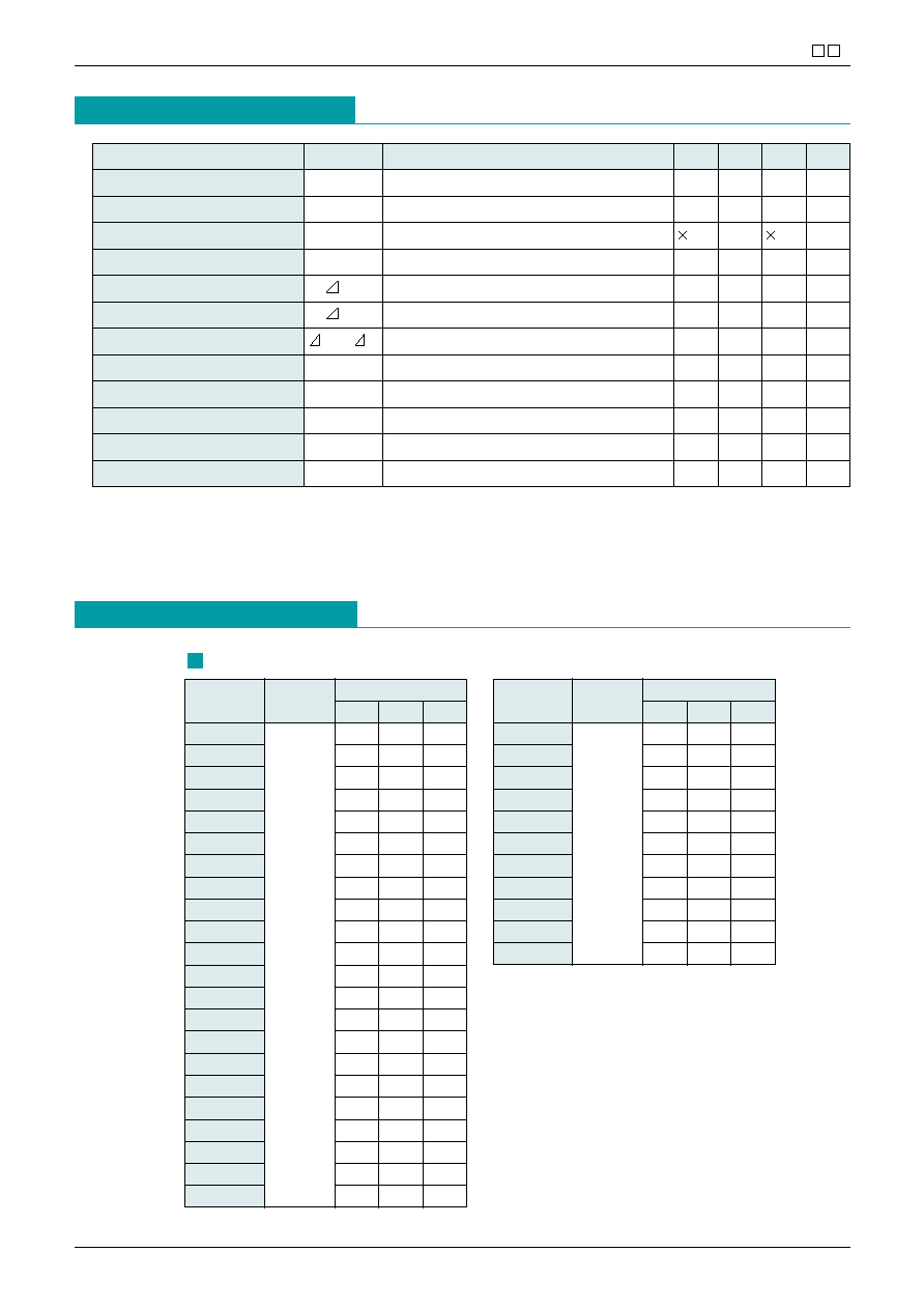
Absolute Maximum Ratings
(Ta=25∞C)
Item
Symbol
Ratings
Units
Storage temperature
T
STG
-40~+150
∞C
Supply voltage
V
IN
-0.3~+12
V
Allowable loss
Pd
400 (Not attached)
mW
950 (
*
1)
Recommended Operating Conditions
Item
Symbol
Ratings
Units
Operating temperature
T
OPR
-30~+85
∞C
Output current
I
OUT
0~500
mA
Operating voltage
V
OP
V
O
Typ.+0.5~+10
V
*
1 With the double sided PC Board of glass epoxy
(Copper plane 80%, 192 142 1.2mm)

MITSUMI
500mA Regulator MM156 F
Electrical Characteristics 1
(Except where noted therwise, Ta=25∞C, V
CC
=9V)
Electrical Characteristics 2
Item
Symbol
Measurement conditions
Min. Typ. Max. Units
No-Load input current
I
CC
Io=0mA
1.9
5
mA
Input current (OFF)
I
CCOFF
V
CONT
=0V
0
1
µA
Output voltage
*
3
V
OUT
Io=250mA
0.98
1.02
V
Dropout voltage
*
4
V
IO
V
IN
=V
O
-0.2V, I
O
=250mA
0.3
0.5
V
Line regulation
V1
V
IN
=V
O
+1.5~Vo+2.5V, I
O
=250mA
10
20
mV
Load regulation
V2
Io=0~250mA
20
120
mV
V
OUT
temperature coefficient
*
2
V
OUT
/ T
Tj=-30~+85∞C
100
ppm/∞C
Ripple rejection
*
2
RR
f=120Hz V
RIPPLE
=1V, I
O
=250mA
50
64
dB
Output noise voltage
*
2
Vn
fBW=20~80kHz Cn=470pF
75
µVrms
CONT pin input current
I
CONT
V
CONT
=V
IN
10
20
30
µA
CONT pin high threshold level
V
CONT
H
1.6
V
IN
+0.3
V
CONT pin low threshold level
V
CONT
L
-0.3
0.4
V
*
2. The parameter is guaranteed by design.
*
3. Please refer to another page.
*
4. The parameter is not guaranteed in the model less than V
OUT
=2V.
Product
Test Output
voltage
name
condisions Min. Typ. Max.
MM1561J
1.764 1.8
1.836
MM1561K
1.862 1.9 1.938
MM1562A
1.960 2.0 2.040
MM1562B
2.058 2.1 2.142
MM1562C
2.156 2.2 2.244
MM1562D
2.254 2.3 2.346
MM1562E
2.352 2.4 2.448
MM1562F
2.450 2.5 2.550
MM1562G
2.548 2.6 2.652
MM1562H
2.646 2.7 2.754
MM1562J
2.744 2.8 2.856
MM1562K
2.842 2.9 2.958
MM1563A
2.940 3.0 3.060
MM1563B
3.038 3.1 3.162
MM1563C
3.136 3.2 3.264
MM1563D
3.234 3.3 3.366
MM1563E
3.332 3.4 3.468
MM1563F
3.430 3.5 3.570
MM1563G
3.528 3.6 3.672
MM1563H
3.626 3.7 3.774
MM1563J
3.724 3.8 3.876
MM1563K
3.822 3.9 3.978
Io=250mA
Product
Test Output
voltage
name
condisions Min. Typ. Max.
MM1564A
3.920 4.0 4.080
MM1564B
4.018 4.1 4.182
MM1564C
4.116 4.2 4.284
MM1564D
4.214 4.3 4.386
MM1564E
4.312 4.4 4.488
MM1564F
4.410 4.5 4.590
MM1564G
4.508 4.6 4.692
MM1564H
4.606 4.7 4.794
MM1564J
4.704 4.8 4.896
MM1564K
4.802 4.9 4.998
MM1565A
4.900 5.0 5.100
Io=250mA
Output Voltage

MITSUMI
500mA Regulator MM156 F
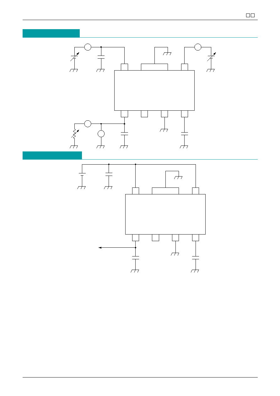
Measuring Circuit
NC
1
2
GND
3
Sub
V
IN
6
Cn
4
Cont
5
O
V
7
V
A
A
A
C
IN
=1
µ
F
Ceramic
Co=2.2
µ
F
Ceramic
*
Ceramic
Cn=470pF
Application Circuit
NC
1
2
GND
3
Sub
V
IN
6
Cn
4
Cont
5
O
V
7
C
IN
=1
µ
F
Ceramic
Co=2.2
µ
F
Ceramic
*
Ceramic
Cn=470pF
Input
To load
Note
1. The output capacitor is required between output and GND to prevent oscillation.
2. Use a capacitance that is within the ESR characteristics stable range for output capacity.
It is possible to use a ceramic capacitor without ESR resistance for output.
The ceramic capacitor must be used more than 2.2µF and B type temperature characteristics.
3. The wire of Vcc and GND is required to print full ground plane for noise and stability.
4. The input capacitor must be connected a distance of less than 1cm from input pin.
5. The capacitor is connected to Cn must have low leakage current characteristics, because Cn pin is high
impedance.
6. The 6pin (heat sink pin) must be connected to GND. This pin can be only connected to GND.
7. In case the output voltage is above the input voltage, the overcurrent flow by internal parasitic diode from
output to input. In such application, the external bypass diode must be connected between output and
input pin.
*
Temperature Characteristics: B Type
