 | –≠–ª–µ–∫—Ç—Ä–æ–Ω–Ω—ã–π –∫–æ–º–ø–æ–Ω–µ–Ω—Ç: MM1574G | –°–∫–∞—á–∞—Ç—å:  PDF PDF  ZIP ZIP |

MITSUMI
150mA Regulator MM157 N, 161 N
150mA Regulator
Monolithic IC MM157 N, 161 N
Outline
This IC is an ultra-small, low noise, stable power supply that supports ceramic capacitors (low ESR) Output
current goes up to 150mA, and use of a noise pin reduces output noise even further.
Output ON/OFF can be controlled with the ON/OFF pin.
Features
1. I/O voltage difference
0.10V typ. (I
O
=50mA)
2. Output noise voltage
30µVrms typ. (Cn=0.01µF)
3. Recommended maximum output current
150mA max.
4. No-load current consumption
85µA typ.
5. Built-in overcurrent protection and thermal shutdown circuits
6. Output voltage rank
1.8 ~ 5.0V (0.1V steps)
7. Output ON/OFF control function
High: ON, Low: OFF
Package
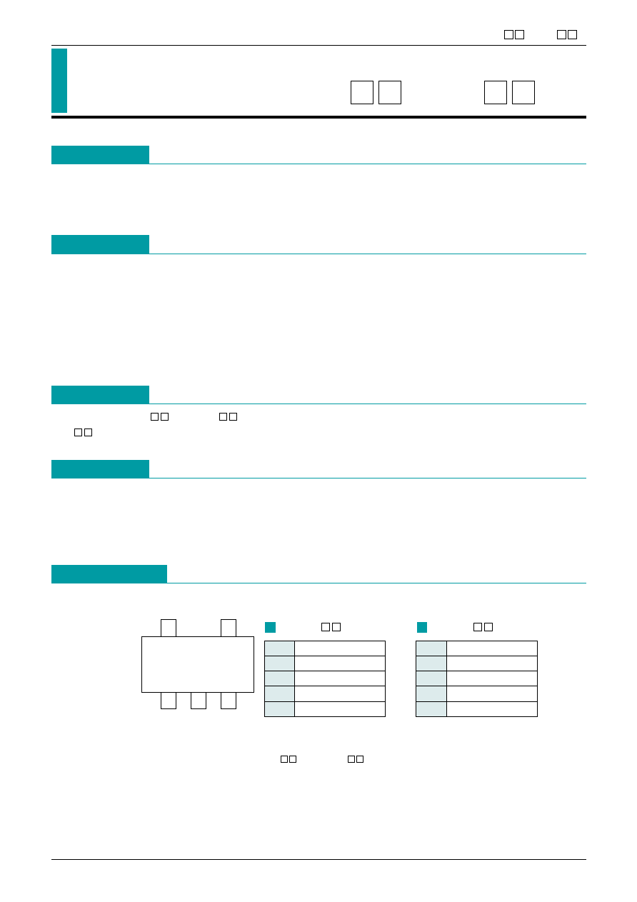
SOT-25A (MM157 N, MM161 N)
*
contains the output voltage rank.
Applications
1. Cordless telephone
2. Cellular telephone, PHS
3. Portable MD
4. Other battery-powered portable equipment
1
3
5
2
4
SOT-25A
(TOP VIEW)
1
V
IN
2
GND
3
Cont
4
Noise
5
V
O
Pin Assignment
MM157 N
1
Cont
2
GND
3
Noise
4
V
OUT
5
V
IN
MM161 N
*
The component MM161 N is MM157 N with changed pin configuration.

MITSUMI
150mA Regulator MM157 N, 161 N
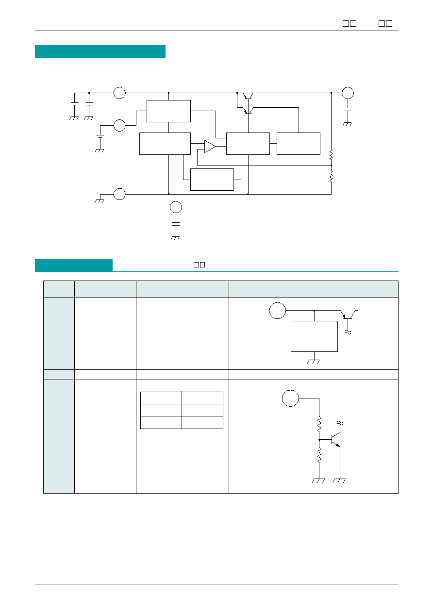
Equivalent Circuit Diagram
GND
V
IN
Bias
Cont
Driver
limitter
Current
Noise
O
V
shutdown
Thermal
Reference
Co
1
µ
F
0.01
µ
F
Cn
1
µ
F
Cin
Pin Description
Typical model: MM157 N
Pin No.
Pin name
Function
Internal equivalent circuit diagram
Input
circuit
1
V
IN
Input pin
The capacitor is required to
connect with input pin
more than 1µF.
2
GND
Ground
3
Cont
ON/OFF Control pin
Cont pin must be
connected with V
IN
pin, if it
is not used.
Cont
V
O
H
ON
L
OFF

MITSUMI
150mA Regulator MM157 N, 161 N
Pin No.
Pin name
Function
Internal equivalent circuit diagram
4
Noise
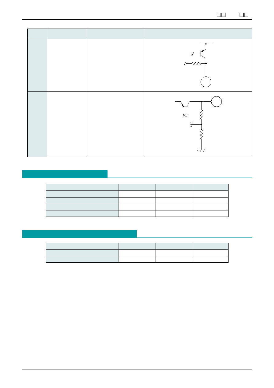
Noise decrease pin
Connecting 0.01µF
capacitor can decrease
output noise. If the noise
decrease capacitor is not
connected, the pin may be
influenced by outside
noise.
5
V
O
Output pin
The capacitor must be
connected with output pin
more than 1µF.
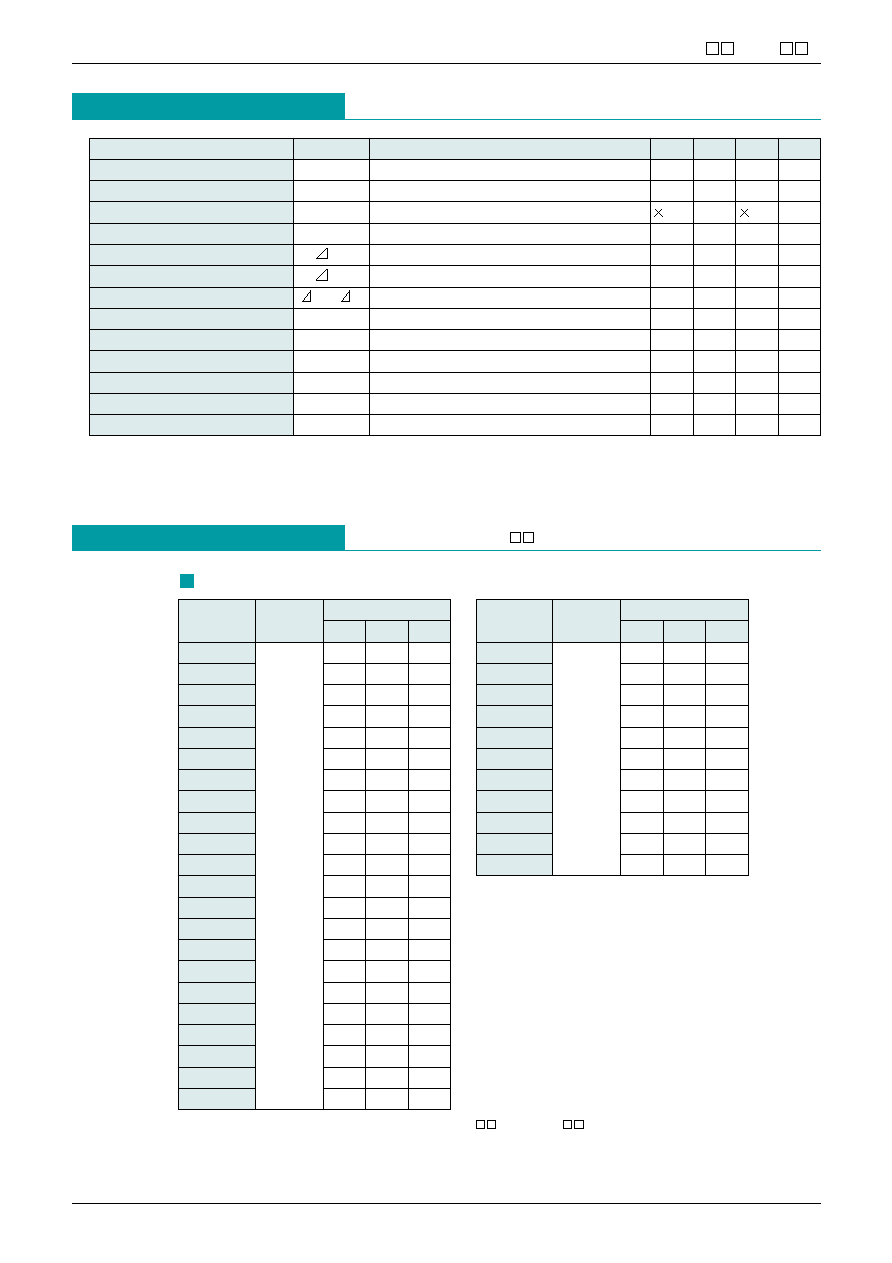
Absolute Maximum Ratings
(Ta=25∞C)
Item
Symbol
Ratings
Units
Storage temperature
T
STG
-40~+150
∞C
Operating temperature
T
OPR
-30~+85
∞C
Supply voltage
V
IN
-0.3~+12
V
Allowable loss
Pd
150 (Not attached)
mW
Recommend
Recommended Operating Conditions
Item
Symbol
Ratings
Units
Output current
I
OUT
0~150
mA
Operating voltage
V
OP
V
OUT
Typ. +0.5~+12
V

MITSUMI
150mA Regulator MM157 N, 161 N
Electrical Characteristics 1
(Except where noted therwise, Ta=25∞C, V
IN
=V
O
Typ. +1V, I
O
=1mA, V
CONT
=2V)
Electrical Characteristics 2
Typical model: MM157 N
Item
Symbol
Measurement conditions
Min. Typ. Max. Units
No-Load input current
I
CC
I
O
=0mA
85
130
µA
Input current (OFF)
I
CCOFF
V
CONT
=0V
0
0.1
µA
Output voltage
V
OUT
0.98
1.02
V
Dropout voltage
*
2
Vio
V
IN
=V
O
-0.2V, I
O
=50mA
0.1
0.2
V
Line regulation
V1
V
IN
=V
O
Typ. +1~10V
10
20
mV
Load regulation
V2
I
O
=1~150mA
30
90
mV
V
OUT
temperature coefficient
*
1
V
OUT
/ T
Tj=-30~+85∞C
100
ppm/∞C
Ripple rejection 1
*
1
RR1
f=120Hz V
RIPPLE
=1V
50
70
dB
Ripple rejection 2
*
1
RR2
f=1kHz, Cn=0.01µF V
RIPPLE
=1V
60
dB
Output noise voltage
*
1
Vn
fBW=20~80kHz Cn=0.01µFC
30
µVrms
Cont pin input current
I
CONT
V
CONT
=5V
5
15
µA
Cont pin high threshold level
V
CONT
H
1.6
V
IN
+0.3
V
Cont pin low threshold level
V
CONT
L
-0.3
0.4
V
*
1. The parameter is guaranteed by design.
*
2. The parameter is not guaranteed in the model less than V
OUT
=2V
Product
Test Output
voltage
name
condisions Min. Typ. Max.
MM1571J
1.764 1.8
1.836
MM1571K
1.862 1.9 1.938
MM1572A
1.960 2.0 2.040
MM1572B
2.058 2.1 2.142
MM1572C
2.156 2.2 2.244
MM1572D
2.254 2.3 2.346
MM1572E
2.352 2.4 2.448
MM1572F
2.450 2.5 2.550
MM1572G
2.548 2.6 2.652
MM1572H
2.646 2.7 2.754
MM1572J
2.744 2.8 2.856
MM1572K
2.842 2.9 2.958
MM1573A
2.940 3.0 3.060
MM1573B
3.038 3.1 3.162
MM1573C
3.136 3.2 3.264
MM1573D
3.234 3.3 3.366
MM1573E
3.332 3.4 3.468
MM1573F
3.430 3.5 3.570
MM1573G
3.528 3.6 3.672
MM1573H
3.626 3.7 3.774
MM1573J
3.724 3.8 3.876
MM1573K
3.822 3.9 3.978
I
O
=1mA
Product
Test Output
voltage
name
condisions Min. Typ. Max.
MM1574A
3.920 4.0 4.080
MM1574B
4.018 4.1 4.182
MM1574C
4.116 4.2 4.284
MM1574D
4.214 4.3 4.386
MM1574E
4.312 4.4 4.488
MM1574F
4.410 4.5 4.590
MM1574G
4.508 4.6 4.692
MM1574H
4.606 4.7 4.794
MM1574J
4.704 4.8 4.896
MM1574K
4.802 4.9 4.998
MM1575A
4.900 5.0 5.100
I
O
=1mA
*
Rank is indicated inside for MM161 N.
Example: MM1613N is 3.9V typ.
Output Voltage

MITSUMI
150mA Regulator MM157 N, 161 N
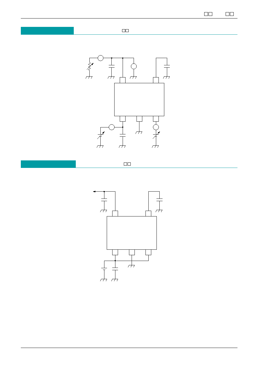
Measuring Circuit
Typical model: MM157 N
1
2
GND
3
V
O
Cont
Noise
IN
V
A
A
Ceramic
*
1
µ
F
1
µ
F
Ceramic
*
5
4
V
Ceramic
0.01
µ
F
A
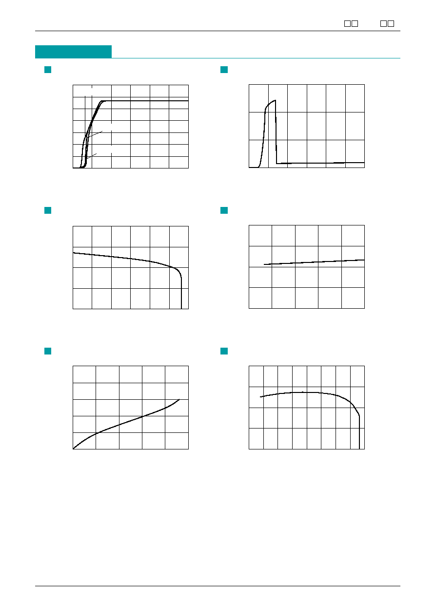
Application Circuit
Typical model: MM157 N
1
2
GND
3
V
O
Cont
Noise
IN
V
Ceramic
*
1
µ
F
1
µ
F
Ceramic
*
5
4
Ceramic
0.01
µ
F
Note
1. The output capacitor is required between output and GND to prevent oscillation.
2. Use a capacitance that is within the ESR characteristics stable range for output capacity.
It is possible to use a ceramic capacitor without ESR resistance for output.
The ceramic capacitor must be used more than 1µF and B type temperature characteristics.
3. The wire of Vcc and GND is required to print full ground plane for noise and stability.
4. The input capacitor must be connected a distance of less than 1cm from input pin.
*
Temperature Characteristics: B Type

MITSUMI
150mA Regulator MM157 N, 161 N
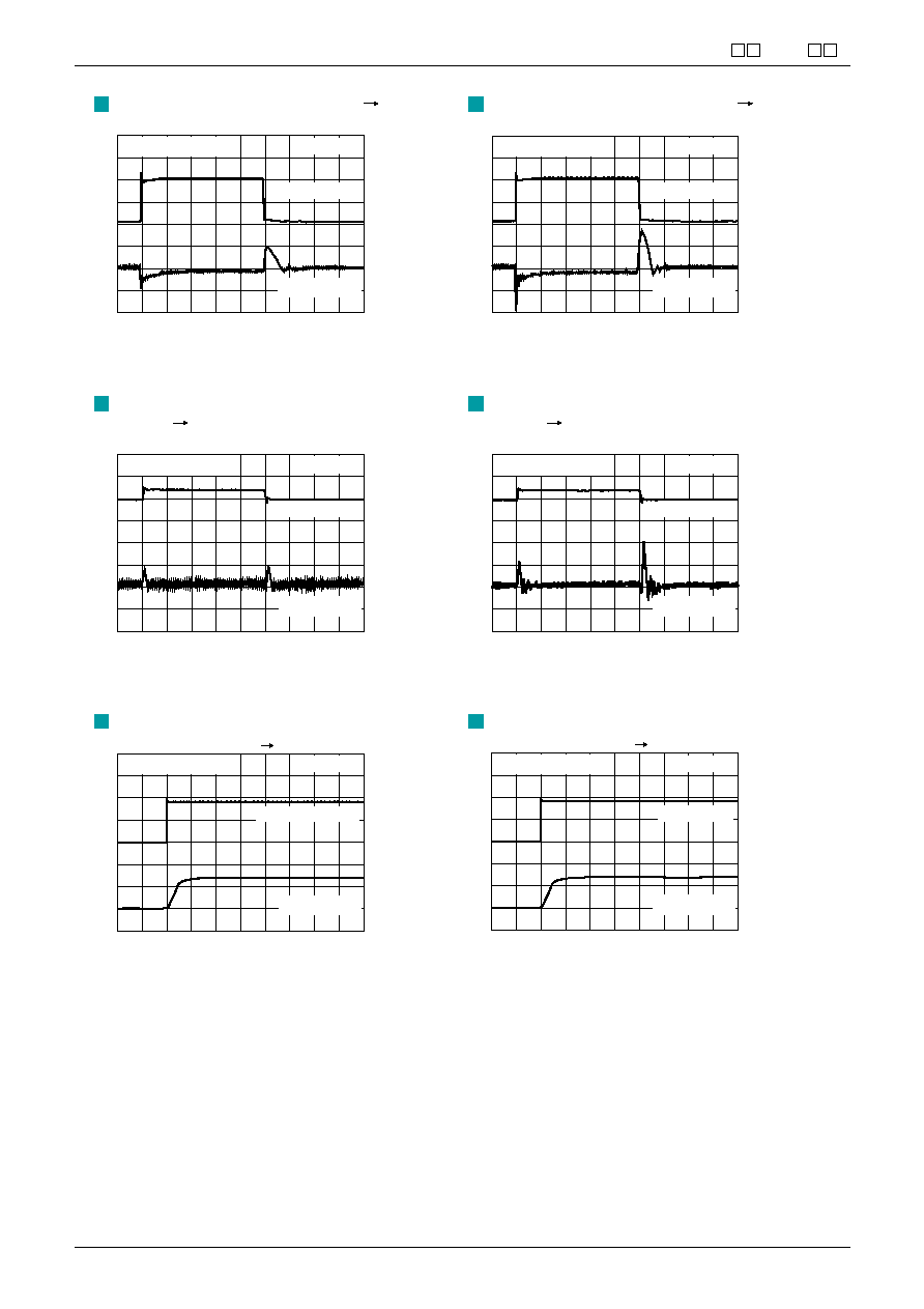
Characteristics
(2.8V product Except where noted therwise, Ta=25∞C, V
IN
=V
O
+1V, V
CONT
=2V, C
IN
=1µF, Co=1µF, Cn=0.01µF)
Output-Input Voltage
Input Current-Input Voltage
0.0
8
2
12
10
4
6
0
Input Voltage V
IN
(V)
2.0
0.5
1.0
1.5
2.5
3.5
3.0
Output Voltage V
O
(V)
R
L
=2.8k
R
L
=93
R
L
=19
0.0
8
10
12
2
4
6
0
Input Voltage V
IN
(V)
1.0
0.5
1.5
Input Current I
IN
(mA)
R
L
=
Load Regulation
2.70
200
250
300
50
100
150
0
Output Current I
O
(mA)
2.80
2.75
2.90
2.85
Output Voltage V
O
(V)
Line Regulation
Dropout Voltage-Output Current
2.825
8
12
10
4
6
2
Input Voltage V
IN
(V)
2.835
2.830
2.845
2.840
Output Voltage V
O
(V)
R
L
=2.8k
0
150
200
250
50
100
0
Output Current I
O
(mA)
0.3
0.2
0.1
0.5
0.4
Dropout Voltage V
IO
(V)
V
IN
=2.6V
Output Voltage- Ambient Temperature
2.70
75 100
-25
150
125
0
25
50
-50
Ambient Temperature Ta (
∞
C)
2.80
2.75
2.90
2.85
Output Voltage V
O
(V)
R
L
=2.8k

MITSUMI
150mA Regulator MM157 N, 161 N
Ripple Rejection
Ripple Rejection
-80
10
1000
100
0.1
1
0.01
Frequency f (kHz)
-20
-30
-40
-50
-60
-70
0
-10
Ripple Rejection RR (dB)
Cn=0.01
µ
F
I
O
=150mA I
O
=100mA
I
O
=30mA
-80
10
1000
100
0.1
1
0.01
Frequency f (kHz)
-20
-30
-40
-50
-60
-70
0
-10
Ripple Rejection RR (dB)
Cn=0
I
O
=150mA
I
O
=100mA
I
O
=30mA
GND Pin Current
0
150
200
250
50
100
0
Output Current I
O
(mA)
10
15
20
5
30
25
GND Pin Current I
CC
(mA)
Output Noise Voltage
ESR Stability Area
0
0.01
0.1
0.0001
0.001
0.00001
Noise Reduction Capacitor Cn (
µ
F)
100
50
200
150
Output Noise Voltage Vn (
µ
Vrms)
150
250
50
100
0
C
IN
=C
O
=1
µ
F
0.01
Output Current I
O
(mA)
1
0.1
10
ESR (
)
200
Stable area
ESR Stability Area
150
250
50
100
0
C
IN
=C
O
=0.47
µ
F
0.01
Output Current I
O
(mA)
1
0.1
10
ESR (
)
200
Stable area

MITSUMI
150mA Regulator MM157 N, 161 N
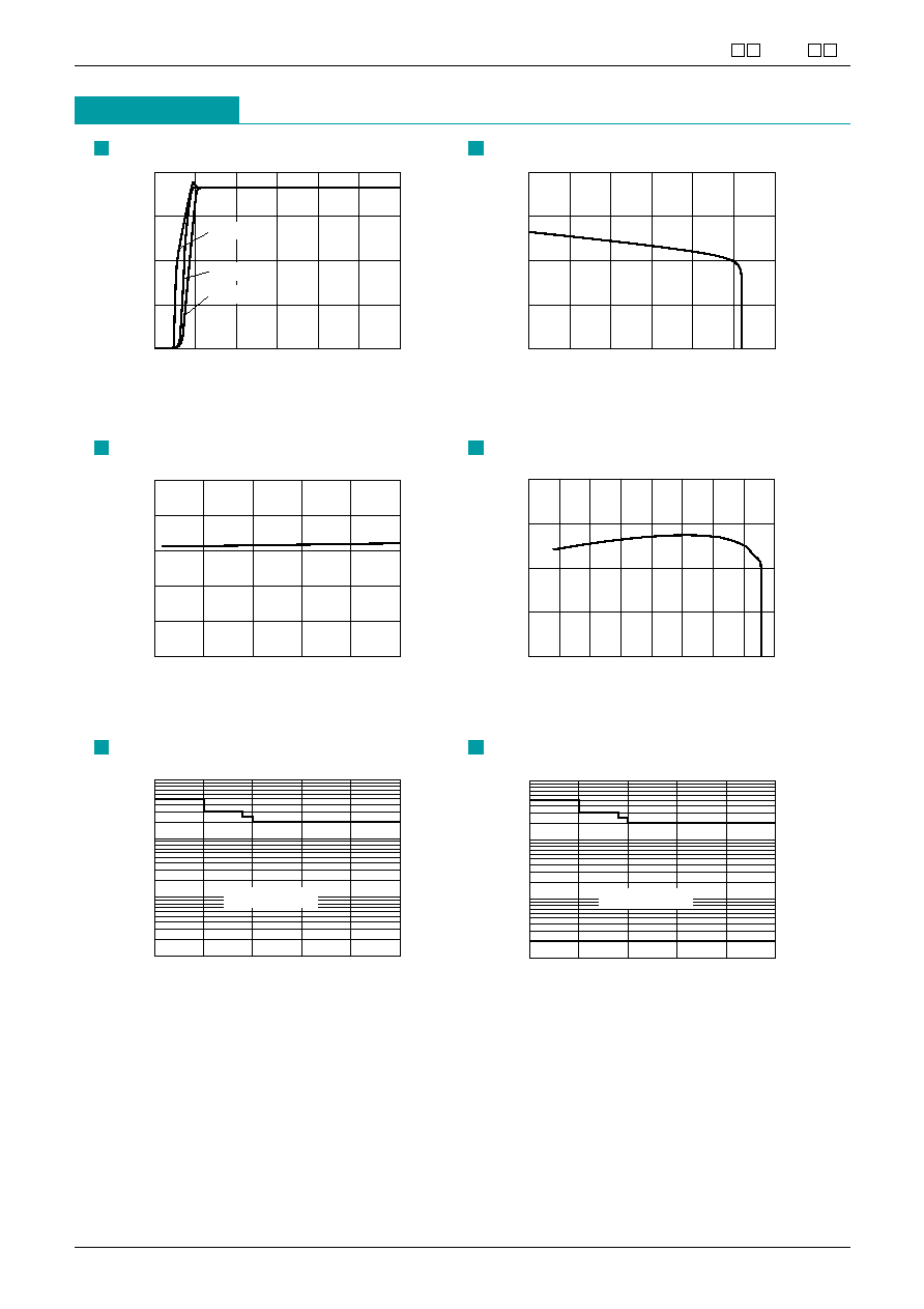
Load Transient Respones (I
O
=0 100mA)
Load Transient Respones (I
O
=0 100mA)
C
IN
=C
O
=1
µ
F, Cn=0.01
µ
F
CH1=10mV
DC 1 : 1
CH2=50mV
AC 10 : 1
100mA
GND
10
µ
s/div
I
O
: 50mA/div
V
O
: 50mV/div
C
IN
=C
O
=0.47
µ
F, Cn=0.01
µ
F
CH1=10mV
DC 1 : 1
CH2=50mV
AC 10 : 1
100mA
GND
10
µ
s/div
I
O
: 50mA/div
V
O:
50mV/div
Line Transient Respones
(V
IN
=3.8 4.8V, I
O
=30mA)
C
IN
=0, C
O
=1
µ
F, Cn=0.01
µ
F
CH1=2V
DC 1 : 1
CH2=20mV
AC 10 : 1
4V
GND
10
µ
s/div
V
IN
: 2V/div
V
O
: 20mV/div
Line Transient Respones
(V
IN
=3.8 4.8V, I
O
=30mA)
Turn-On Transient Respones
C
IN
=0, C
O
=0.47
µ
F, Cn=0.01
µ
F
CH1=2V
DC 1 : 1
CH2=20mV
AC 10 : 1
4V
GND
10
µ
s/div
V
IN
: 2V/div
V
O
: 20mV/div
V
IN
=V
CONT
=0 3.8V, I
O
=30mA
CH1=2V
DC 10 : 1
CH2=2V
DC 10 : 1
4V
4V
GND
GND
100
µ
s/div
V
IN
, Cont: 2V/div
V
O
: 2V/div
Turn-On Transient Tespones
V
IN
=3.8V, V
CONT
=0 3.8V, I
O
=30mA
CH1=2V
DC 10 : 1
CH2=2V
DC 10 : 1
4V
4V
GND
GND
100
µ
s/div
Cont: 2V/div
V
O
: 2V/div

MITSUMI
150mA Regulator MM157 N, 161 N
Characteristics
(1.8V product Except where noted therwise, Ta=25∞C, V
IN
=V
O
+1V, V
CONT
=2V, C
IN
=1µF, Co=1µF, Cn=0.01µF)
Output-Input Voltage
Load Regulation
0.0
8
2
12
10
4
6
0
Input Voltage V
IN
(V)
1.0
0.5
2.0
1.5
Output Voltage V
O
(V)
R
L
=1.8k
R
L
=60
R
L
=12
1.70
200
300
250
50
100
150
0
Output Current I
O
(mA)
1.80
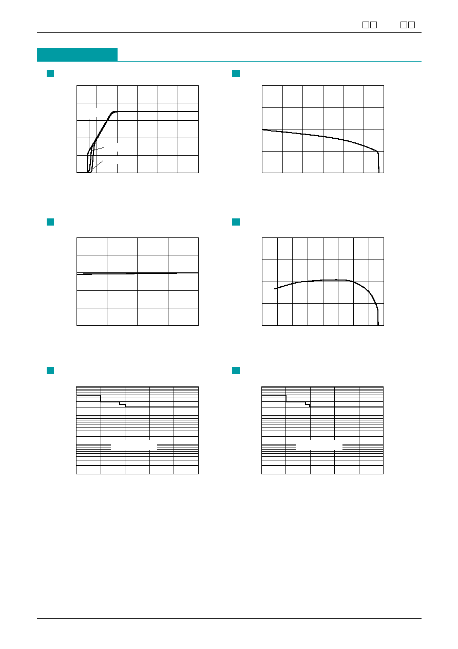
1.75
1.90
1.85
Output Voltage V
O
(V)
Line Regulation
1.80
8
12
10
4
6
2
Input Voltage V
IN
(V)
1.83
1.82
1.81
1.85
1.84
Output Voltage V
O
(V)
R
L
=1.8k
Output Voltage- Ambient Temperature
ESR Stability Area
1.70
75 100
-25
150
125
0
25
50
-50
Ambient Temperature Ta (
∞
C)
1.80
1.75
1.90
1.85
Output Voltage V
O
(V)
R
L
=1.8k
150
250
50
100
0
C
IN
=C
O
=1
µ
F
0.01
Output Current I
O
(mA)
1
0.1
10
ESR (
)
200
Stable area
ESR Stability Area
150
250
50
100
0
C
IN
=C
O
=0.47
µ
F
0.01
Output Current I
O
(mA)
1
0.1
10
ESR (
)
200
Stable area

MITSUMI
150mA Regulator MM157 N, 161 N
Characteristics
(3.5V product Except where noted therwise, Ta=25∞C, V
IN
=V
O
+1V, V
CONT
=2V, C
IN
=1µF, Co=1µF, Cn=0.01µF)
Output-Input Voltage
Load Regulation
0.0
8
2
12
10
4
6
0
Input Voltage V
IN
(V)
2.0
1.0
5.0
3.0
4.0
Output Voltage V
O
(V)
R
L
=3.5k
R
L
=117
R
L
=23
3.40
200
300
250
50
100
150
0
Output Current I
O
(mA)
3.50
3.45
3.60
3.55
Output Voltage V
O
(V)
Line Regulation
3.47
8
12
10
6
4
Input Voltage V
IN
(V)
3.50
3.49
3.48
3.52
3.51
Output Voltage V
O
(V)
R
L
=3.5k
Output Voltage- Ambient Temperature
ESR Stability Area
3.40
75 100
-25
150
125
0
25
50
-50
Ambient Temperature Ta (
∞
C)
3.50
3.45
3.60
3.55
Output Voltage V
O
(V)
R
L
=3.5k
150
250
50
100
0
C
IN
=C
O
=1
µ
F
0.01
Output Current I
O
(mA)
1
0.1
10
ESR (
)
200
Stable area
ESR Stability Area
150
250
50
100
0
C
IN
=C
O
=0.47
µ
F
0.01
Output Current I
O
(mA)
1
0.1
10
ESR (
)
200
Stable area
