 | –≠–ª–µ–∫—Ç—Ä–æ–Ω–Ω—ã–π –∫–æ–º–ø–æ–Ω–µ–Ω—Ç: MM3005K | –°–∫–∞—á–∞—Ç—å:  PDF PDF  ZIP ZIP |

MITSUMI
CMOS Switching Regulator (PWM controlled) MM3005~MM3010
CMOS Switching Regulator (PWM controlled)
Monolithic IC MM3005~MM3010
Outline
This IC is a PWM controlled switching regulator developed using the CMOS process. Low ripple and high
efficiency of 83% typ. (MM3005E) are achieved through PWM control. Further, output voltage is high
precision output ±2.4%.
Features
1. Ultra low consumption current 17.2µA typ. (during operation) (MM3005E)
2. High efficiency 83% typ. (MM3005E)
3. High precision output voltage ±2.4%
4. Wide operating temperature range -30∞C~+85∞C
5. Output voltage 2~5.5V (0.1V can be set in 0.1V steps)
Package
SOT-25A (Mini mold)
Applications
1. Mobile phones, PHS
2. Portable MD
3. Other battery-operated portable equipment
MITSUMI
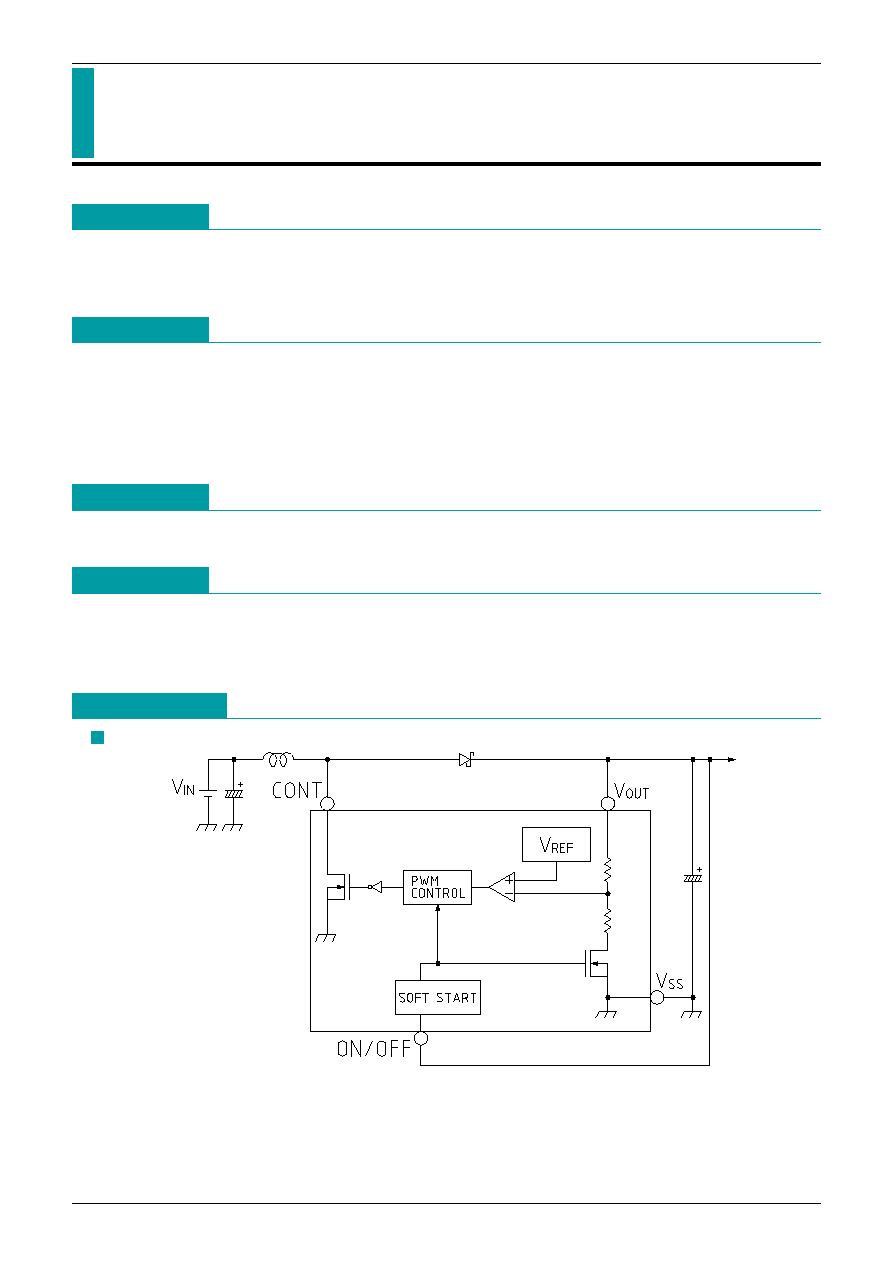
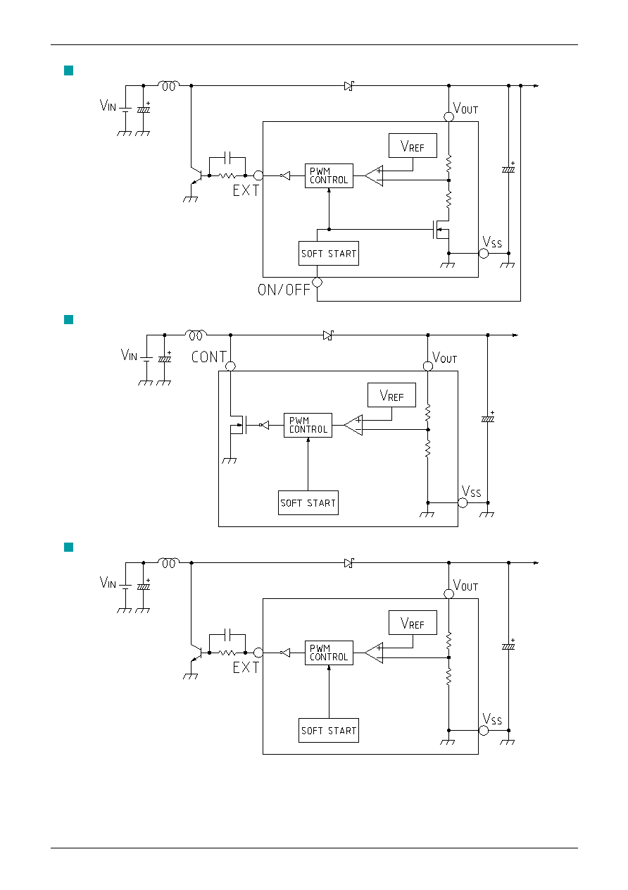
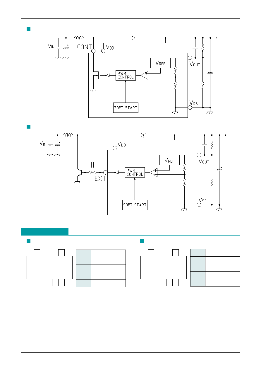
Block Diagram
MM3005

MITSUMI
CMOS Switching Regulator (PWM controlled) MM3005~MM3010
MM3006
MM3007
MM3008

MITSUMI
CMOS Switching Regulator (PWM controlled) MM3005~MM3010
Pin Assignment
MM3009
MM3010
1
3
5
2
4
SOT-25A
(TOP VIEW)
1
ON/OFF
2
V
OUT
3
NC
4
V
SS
5
CONT
1
3
5
2
4
SOT-25A
(TOP VIEW)
1
ON/OFF
2
V
OUT
3
NC
4
V
SS
5
EXT
MM3005
MM3006

MITSUMI
CMOS Switching Regulator (PWM controlled) MM3005~MM3010
1
3
5
2
4
SOT-25A
(TOP VIEW)
1
3
5
2
4
SOT-25A
(TOP VIEW)
MM3007
MM3008
1
3
5
2
4
SOT-25A
(TOP VIEW)
1
3
5
2
4
SOT-25A
(TOP VIEW)
MM3009
MM3010
1
NC
2
V
OUT
3
NC
4
V
SS
5
CONT
1
NC
2
V
OUT
3
NC
4
V
SS
5
EXT
1
V
OUT
2
V
DD
3
NC
4
V
SS
5
CONT
1
V
OUT
2
V
DD
3
NC
4
V
SS
5
EXT
Absolute Maximum Ratings
Item
Symbol
Rating
Unit
Storage Temperature
T
STG
-40~+125 ∞C
Operating Temperature
T
OPR
-30~+85
∞C
Power Supply Voltage
V
DD
max.
-0.3~+11
V
Allowable loss
Pd
150
mW
V
OUT
pin voltage
V
OUT
-0.3~+11
V
ON/OFF pin voltage
ON/OFF
-0.3~+11
V
CONT pin voltage
V
CONT
-0.3~+11
V
CONT pin current
I
CONT
300
mA
Recommended Operating Conditions
Rank expand table
Ta=25∞C
Item
Symbol
Rating
Unit
Operating Temperature
T
OPR
-30~+85
∞C
Input voltage
V
IN
+0.9~+9
V
MM3005A
2.0V±2.4%
MM3005B
2.5V±2.4%
MM3005C
2.7V±2.4%
MM3005D
2.8V±2.4%
MM3005E
3.0V±2.4%
MM3005F
3.3V±2.4%
MM3005G
3.6V±2.4%
MM3005H
5.0V±2.4%
MM3005J
5.2V±2.4%
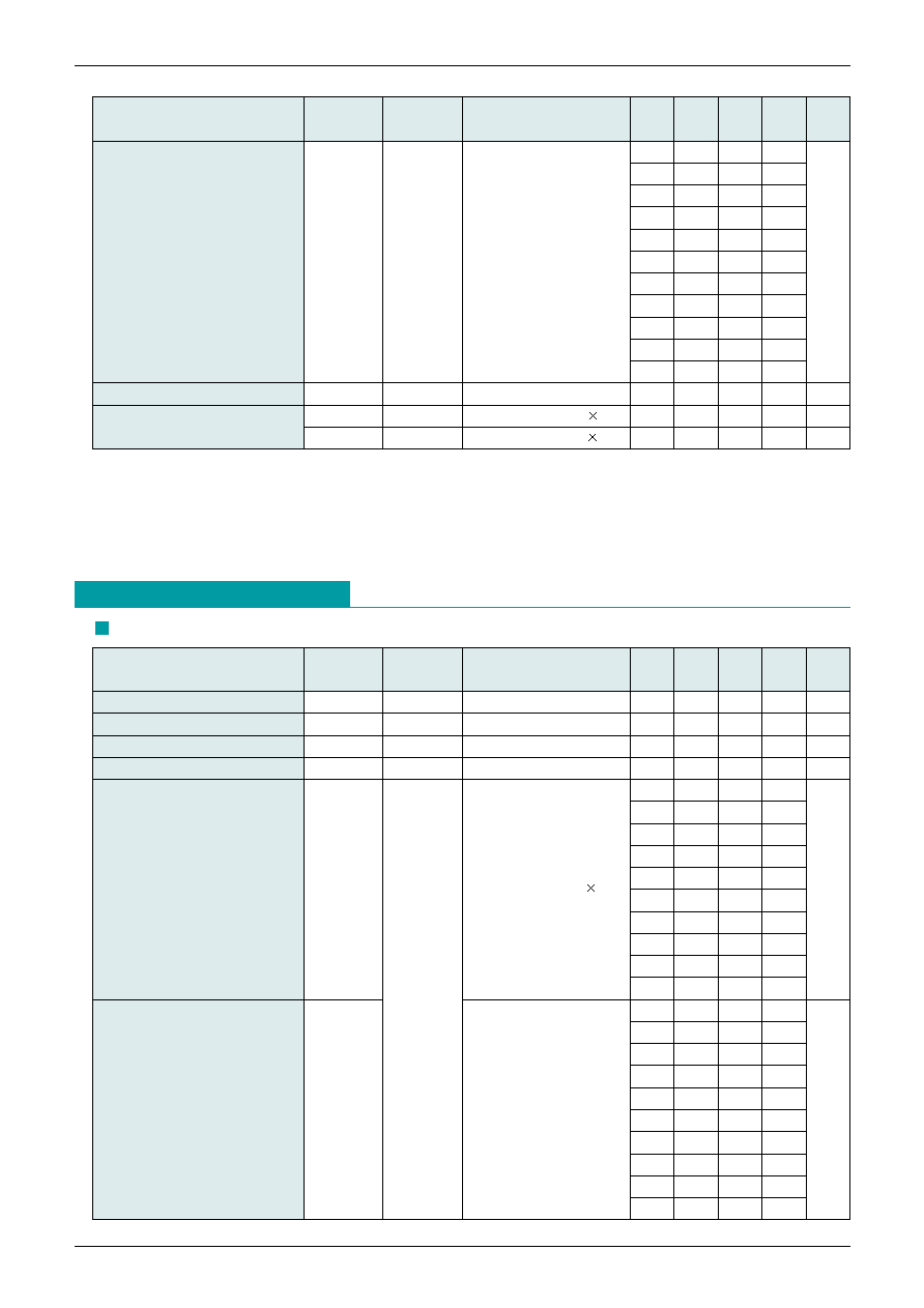
MM3005K
5.4V±2.4%
*
In addition to MM3005, MM3006 ~ MM3010 also have rank indications from A ~ K, as above.

MITSUMI
CMOS Switching Regulator (PWM controlled) MM3005~MM3010
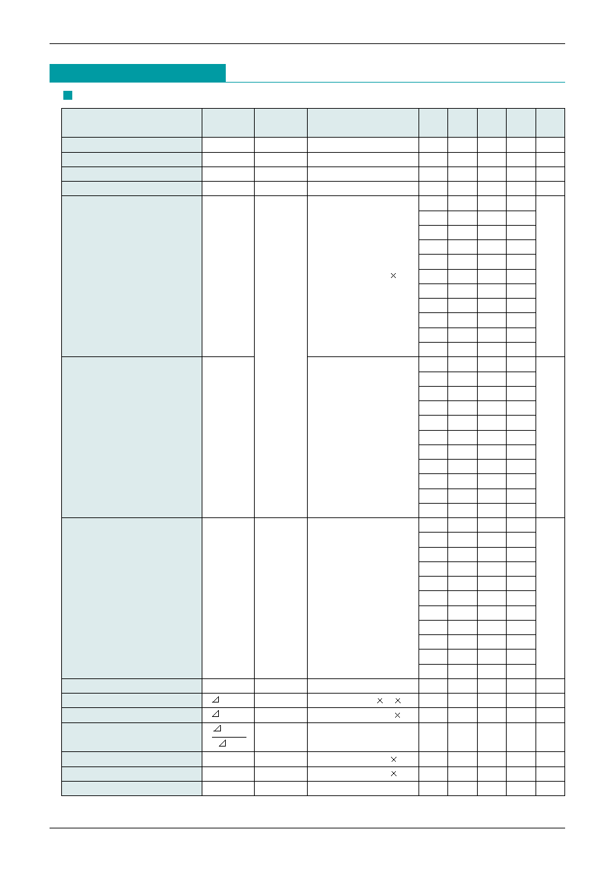
Electrical Characteristics
(Except where noted otherwise, Ta=25∞C)
Item
Symbol
Measurement
Measuring Circuit
Rank Min. Typ. Max. Unit
circuit
Input voltage
V
IN
1
9
V
Operating start voltage
V
ST1
1
I
OUT
=1mA
0.9
V
Oscillation start voltage
V
ST2
2
0.8
V
Operation hold voltage
V
HLD
1
I
OUT
=1mA
0.7
V
A
11.6
19.4
B
14.3
23.9
C
15.5
25.9
D
16.1
26.8
E
17.2
28.7
Consumption current 1
I
SS1
V
OUT
= Output voltage 0.95
F
19.1
31.8
µA
G
22.4
37.3
H
38.5
64.1
J
43.9
73.1
2
K
45.0
74.9
L
13.2
22.8
A
3.1
6.2
B
3.2
6.3
C
3.2
6.4
D
3.2
6.4
E
3.2
6.4
Consumption current 2
I
SS2
V
OUT
= Output voltage+0.5V
F
3.3
6.5
µA
G
3.3
6.5
H
3.5
6.9
J
3.5
6.9
K
3.5
6.9
L
3.1
6.2
A
45
71
B
61
98
C
61
98
D
61
98
E
78
125
mA
Switching current
I
SW
V
CONT
=0.4V
F
78
125
G
78
125
H
114
182
J
114
182
K
114
182
L
45
71
Switching transistor leak current
I
SWO
V
OUT
=V
CONT
=9V
1
µA
Input stability
V
OUT1
1
V
IN
= Output voltage 0.4 0.6
30
60
mV
Load stability
V
OUT2
1
I
OUT
=10µA~I
OUT
(Following) 1.25
30
60
mV
Output voltage
V
OUT
1
Ta= -30~85∞C
±50
ppm/∞C
temperature coefficient
Ta
Oscillation frequency
fosc
2
V
OUT
= Output voltage 0.95
42.5
50
57.5
kHz
Maximum duty ratio
MaxDuty
2
V
OUT
= Output voltage 0.96
75
83
90
%
Soft start
Tss
I
OUT
=1mA
3
6
12
ms
MM3005, MM3007, MM3009 (It is L rank only MM3009.)

MITSUMI
CMOS Switching Regulator (PWM controlled) MM3005~MM3010
MITSUMI
Item
Symbol
Measurement
Measuring Circuit
Rank Min. Typ. Max. Unit
circuit
A
75
B
79
C
79
D
79
E
83
Efficiency
E
FFI
1
F
83
%
G
83
H
87
J
87
K
87
L
75
Consumption current while power off
*
Isss
2
ON/OFF pin=0V
0.5
µA
ON/OFF pin input voltage
V
SH
2
V
OUT
=Output voltage 0.95
0.75
V
V
SL
2
V
OUT
=Output voltage 0.95
0.3
V
Note 1:
*
Consumption current when ON/OFF and power OFF pin input voltage apply only to MM3005.
Note 2: If rank is not filled in, applies to all ranks.
Note 3: I
OUT
=Output voltage/250
Note 4: The V
DD
pin and V
OUT
pin are connected for the V
DD
/V
OUT
separated type.
MM3006, MM3008, MM3010
Electrical Characteristics2
(Except where noted otherwise, Ta=25∞C)
Item
Symbol
Measurement
Measuring Circuit
Rank Min. Typ. Max. Unit
circuit
Input voltage
V
IN
1
9
V
Operating start voltage
V
ST1
1
I
OUT
=1mA
0.9
V
Oscillation start voltage
V
ST2
2
0.8
V
Operation hold voltage
V
HLD
1
I
OUT
=1mA
0.7
V
A
14.5
24.1
B
17.8
29.7
C
19.2
32
D
20
33.3
Consumption current 1
I
SS1
V
OUT
=Output voltage 0.95
E
21.4
35.7
µA
F
23.7
39.5
G
28.8
48
H
54
89.9
J
56.2
93.6
2
K
58.9
98.1
A
3.8
7.6
B
3.9
7.7
C
3.9
7.7
D
3.9
7.8
Consumption current 2
I
SS2
V
OUT
=Output voltage+0.5V
E
3.9
7.8
µA
F
4
7.9
G
4
7.9
H
4.2
8.3
J
4.2
8.3
K
4.2
8.3

MITSUMI
CMOS Switching Regulator (PWM controlled) MM3005~MM3010
Item
Symbol
Measurement
Measuring Circuit
Rank Min. Typ. Max. Unit
circuit
A
-1.9
-2.9
B
-2.7
-4
C
-2.7
-4
D
-2.7
-4
I
EXTH
VEXT=V
OUT
-0.4V
E
-3.5
-5.3
mA
F
-3.5
-5.3
G
-3.5
-5.3
H
-5.3
-8
J
-5.3
-8
EXT pin output current
K
-5.3
-8
A
3.8
5.7
B
5.3
8
C
5.3
8
D
5.3
8
I
EXTL
VEXT=0.4V
E
7
10.5
mA
F
7
10.5
G
7
10.5
H
10.7
16
J
10.7
16
K
10.7
16
Input stability
V
OUT1
3
V
IN
=Output voltage 0.4~ 0.6
30
60
mV
Load stability
V
OUT2
3
I
OUT
=10µA~I
OUT
(Following) 1.25
30
60
mV
Output voltage temperature coefficient
V
OUT
3
Ta=-30~85∞C
±50
ppm/∞C
Ta
Oscillation frequency
fosc
4
V
OUT
=Output voltage 0.95
85
100
115
kHz
Maximum duty ratio
MaxDuty 4
V
OUT
=Output voltage 0.96
75
83
90
%
Soft start
Tss
I
OUT
=1mA
3
6
12
ms
A
76
B
80
C
80
D
80
Efficiency
EFFI
3
E
84
%
F
84
G
84
H
88
J
88
K
88
Consumption current while power off
Isss
4
Power off pin=0V
0.5
µA
ON/OFF pin input voltage
V
SH
4
V
OUT
Output voltage 0.95
0.75
V
V
SL
V
OUT
Output voltage 0.95
0.3
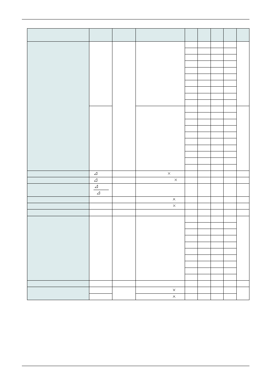
Notes: 1. The current consumption when powering down and input voltage at the ON/OFF pin apply only to
the MM3006.
Notes: 2. Where the rank is omitted, the figure is common to all ranks.
Notes: 3. I
OUT
=output voltage 250
Notes: 4. Connect both V
DD
and V
OUT
pins in models with separate V
DD
and V
OUT
pins.

MITSUMI
CMOS Switching Regulator (PWM controlled) MM3005~MM3010
MITSUMI
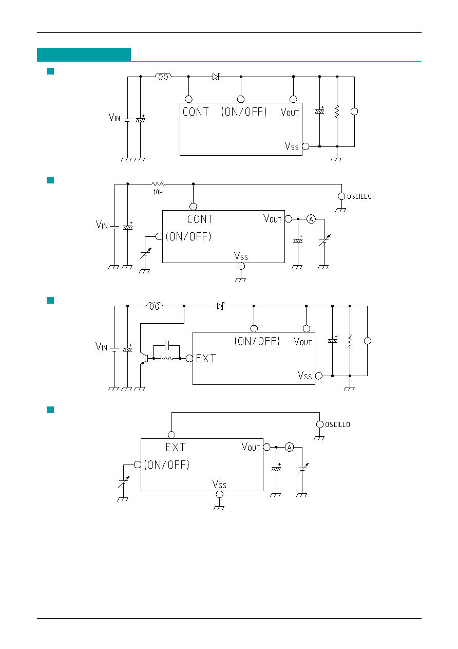
Measuring Circuit
1
2
3
4
Note 1: Coil: L=100µH (Mitsumi C5-K3L) transistor: SANYO 2SD1628
Condenser: C=33µF (tantal condenser) Base resistor (Rb) : 1.0k
Shot key barrier diode: ROHM RB491D Base resistor (Cb) : 2200pF
Note 2: The cause of oscillation is due to set wiring and capacitance changes in capacitor caused by
temperatures changes, so please take extra care in placing the wires.

MITSUMI
CMOS Switching Regulator (PWM controlled) MM3005~MM3010
Description of Operation
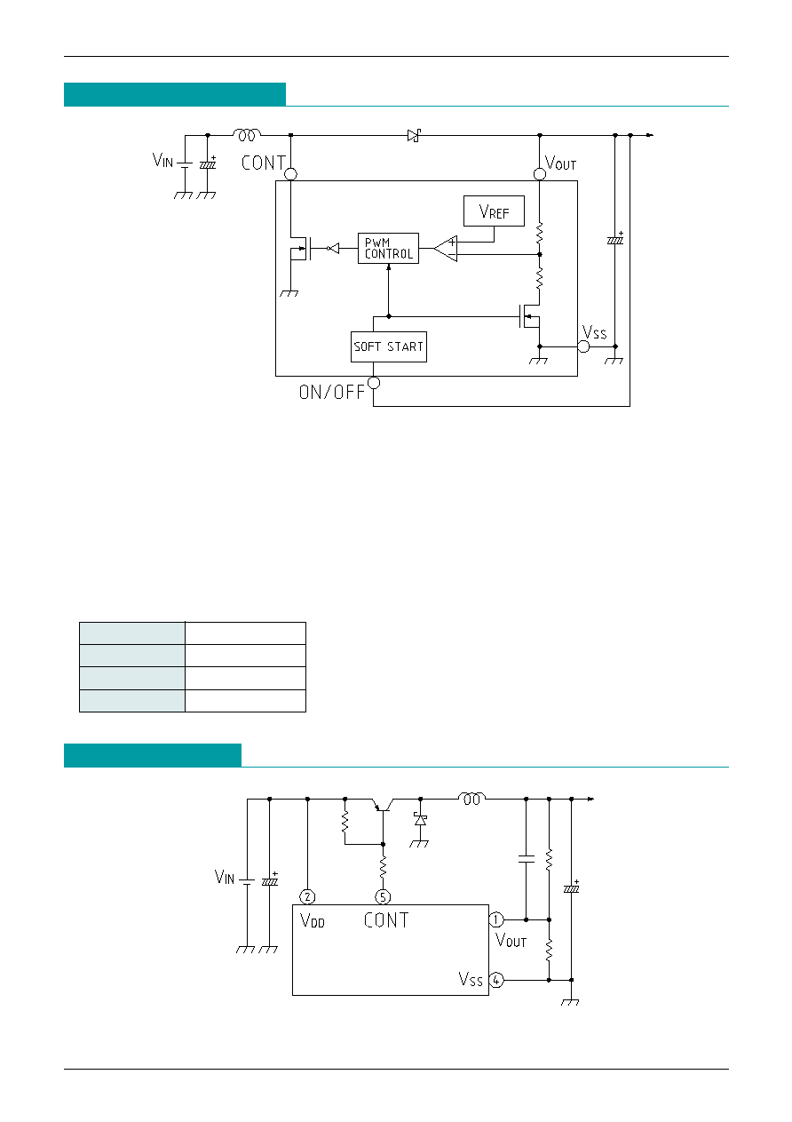
The MM3005 series are pulse width modulation type DC/DC converters.
1: PWM control uses load to change the duty ratio automatically from 0 ~ 83%.
2: A built-in soft start circuit softens the current inrush at start-up.
3: Power OFF pin: Stops or starts voltage rise operation.
When the power OFF pin is at low level the internal circuits all stop operating and consumption current is
greatly reduced. Note that the power OFF pin structure is open and unstable, so please be sure not to use
it open. Further, do not impress voltage of 0.3 ~ 0.75V, as this causes consumption current to increase.
When not using the power OFF pin, please connect it to the V
OUT
pin.
Application Circuits
Power off pin
Operating condition
H
ON
L
OFF
Open
Irregular
When used as voltage drop DC-DC converter.

MITSUMI
CMOS Switching Regulator (PWM controlled) MM3005~MM3010
MITSUMI
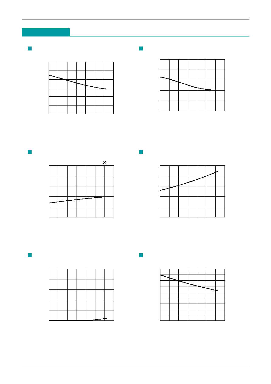
Characteristics
MM3005EN Output voltage3V typ. product
0.0
0.2
0.4
0.6
0.8
1.0
-40 -20
0
20
40
60
80
100
1.2
I
OUT
=1mA
Ta (
∞
C)
V
ST1
(V)
0.0
0.2
0.4
0.6
0.8
1.0
Ta (
∞
C)
V
ST2
(V)
-40 -20
0
20
40
60
80
100
Starting output voltage vs temperature
Starting oscillator voltage vs temperature
0
10
20
30
40
50
V
OUT
=Output Voltage 0.95
Ta (
∞
C)
I
SS1
(
µ
A)
-40 -20
0
20
40
60
80
100
0
1
2
3
4
5
V
OUT
=Output Voltage+0.5
Ta (
∞
C)
I
SS2
(
µ
A)
-40 -20
0
20
40
60
80
100
Supply current 1 vs temperature
Supply current 2 vs temperature
0.0
0.2
0.4
0.6
0.8
1.0
ON/OFF pin=0V
Ta (
∞
C)
I
SSS
(
µ
A)
-40 -20
0
20
40
60
80
100
Supply current (OFF) vs temperature
0
25
50
75
100
125
150
175
200
255
V
CONT
=0.4V
Ta (
∞
C)
I
SW
(mA)
-40 -20
0
20
40
60
80
100
Switch current vs temperature
Note: these are typical characteristics.

MITSUMI
CMOS Switching Regulator (PWM controlled) MM3005~MM3010
0.0
0.2
0.4
0.6
0.8
1.0
V
OUT
=V
CONT
=10V
Ta (
∞
C)
I
SWQ
(
µ
A)
-40 -20
0
20
40
60
80
100
30
35
40
45
50
55
60
65
70
V
OUT
=Output Voltage 0.95
Ta (
∞
C)
f
OSC
(kHz)
-40 -20
0
20
40
60
80
100
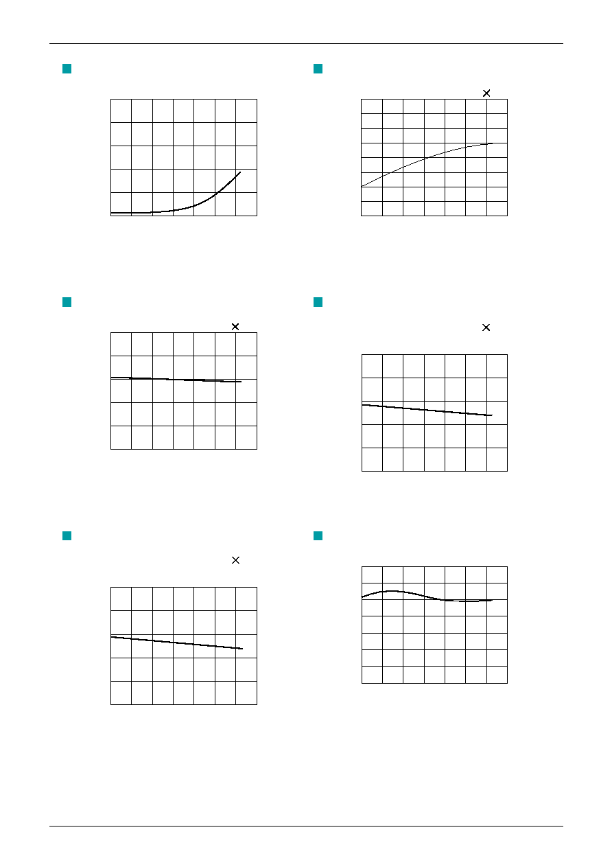
Switch transistor leak current vs temperature
Oscillator frequency vs temperature
50
60
70
80
90
100
V
OUT
=Output Voltage 0.95
Ta (
∞
C)
MaxDuty (%)
-40 -20
0
20
40
60
80
100
0.0
0.2
0.4
0.6
0.8
1.0
V
OUT
=Output Voltage 0.95
The oscillation waveform of
CONT PIN is measured.
Ta (
∞
C)
V
SH
(V)
-40 -20
0
20
40
60
80
100
Maximum duty cycle vs temperature
ON/OFF Pin input voltage (V
SH
) vs temperature
0.0
0.2
0.4
0.6
0.8
1.0
V
OUT
=Output Voltage 0.95
The oscillation stop of
CONT PIN is measured.
Ta (
∞
C)
V
SL
(V)
-40 -20
0
20
40
60
80
100
ON/OFF Pin input voltage (V
SL
) vs temperature
0
2
4
6
8
10
12
14
I
OUT
=1mA
Ta (
∞
C)
T
SS
(ms)
-40 -20
0
20
40
60
80
100
Soft start time vs temperature
Note: these are typical characteristics.

MITSUMI
CMOS Switching Regulator (PWM controlled) MM3005~MM3010
0
50
40
30
20
10
Ta=25
∞
C
V
OUT
(V)
I
SS1
,
2
(
µ
A)
0
2
4
6
8
10
0
250
200
150
100
50
Ta=25
∞
C, V
CONT
=0.4V
V
OUT
(V)
I
SW (
mA)
0
5
4
3
2
1
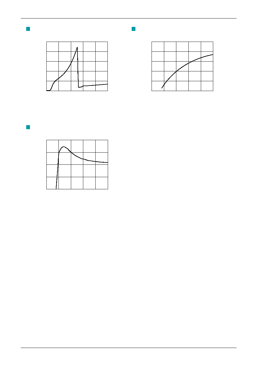
Supply Current 1, 2 vs V
OUT
Switch current vs V
OUT
30
40
50
60
70
Ta=25
∞
C
V
OUT
(V)
f
OSC
(kHz)
0
5
4
3
2
1
Oscillator frequency vs V
OUT
Note: these are typical characteristics.

MITSUMI
CMOS Switching Regulator (PWM controlled) MM3005~MM3010
V
IN
=1.8V
t (10
µ
s/div)
Output
Voltage
V
OUT
(20mV/div)
CONT Voltage
V
CONT
(1V/div)
V
IN
=1.8V
t (10
µ
s/div)
Output
Voltage
V
OUT
(20mV/div)
CONT Voltage
V
CONT
(1V/div)
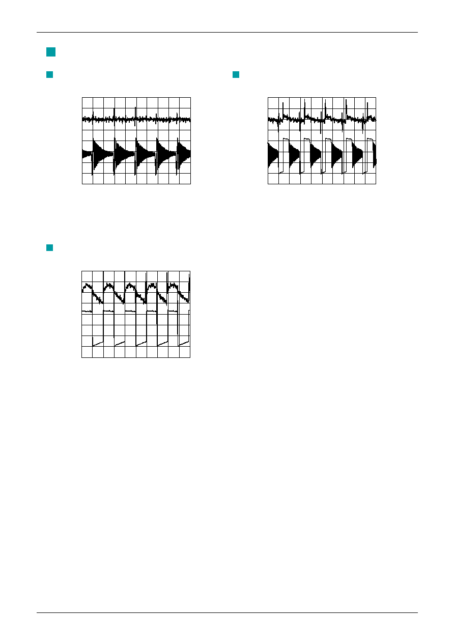
1. I
OUT
=200µA
Ripple voltage characteristic (MM3005EN)
2. I
OUT
=10mA
V
IN
=1.8V
t (10
µ
s/div)
Output
Voltage
V
OUT
(20mV/div)
CONT Voltage
V
CONT
(1V/div)
3. I
OUT
=60mA
Note: these are typical characteristics.

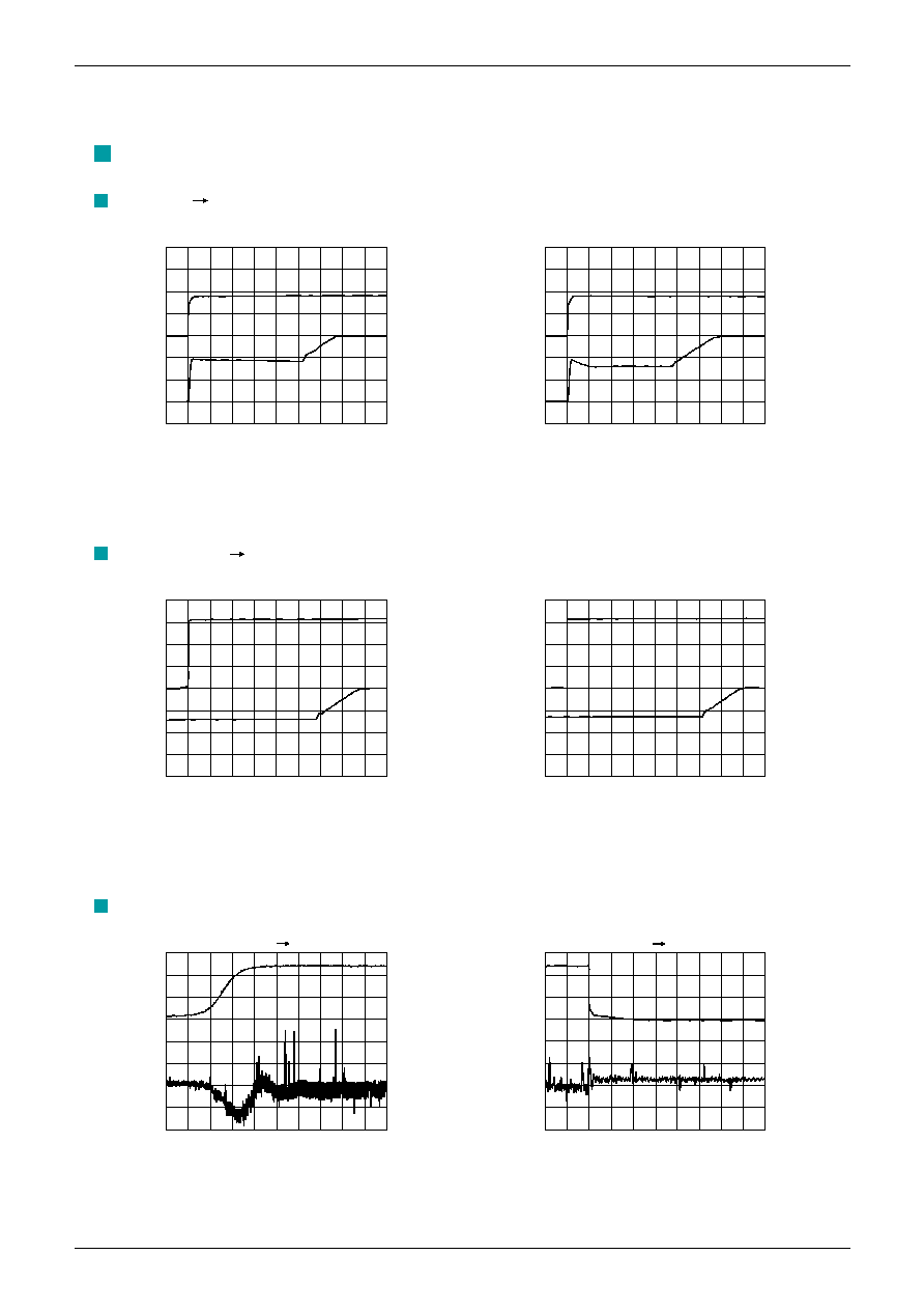
MITSUMI
CMOS Switching Regulator (PWM controlled) MM3005~MM3010
I
OUT
=1mA
t (1ms/div)
Input
Voltage
V
IN
(1V/div)
Output
Voltage
V
OUT
(1V/div)
I
OUT
=60mA
t (1ms/div)
Input
Voltage
V
IN
(1V/div)
Output
Voltage
V
OUT
(1V/div)
1. V
IN
: 0V 1.8V
I
OUT
=1mA, V
IN
=1.8V
t (1ms/div)
Input
Voltage
V
ON/OFF
(1V/div)
Output
Voltage
V
OUT
(1V/div)
I
OUT
=60mA, V
IN
=1.8V
t (1ms/div)
Input
Voltage
V
ON/OFF
(1V/div)
Output
Voltage
V
OUT
(1V/div)
2. V
ON/OFF
: 0V 3.0V
I
OUT
: 100
µ
A 50mA, V
IN
=1.8V
t (200
µ
s/div)
Load
Current
I
OUT
(20mA/div)
Output
Voltage
V
OUT
(50mV/div)
3. Load regulation
I
OUT
: 50mA 100
µ
A, V
IN
=1.8V
t (5ms/div)
Load
Current
I
OUT
(20mA/div)
Output
Voltage
V
OUT
(50mV/div)
Transient Response (MM3005EN)
Note: these are typical characteristics.

MITSUMI
CMOS Switching Regulator (PWM controlled) MM3005~MM3010
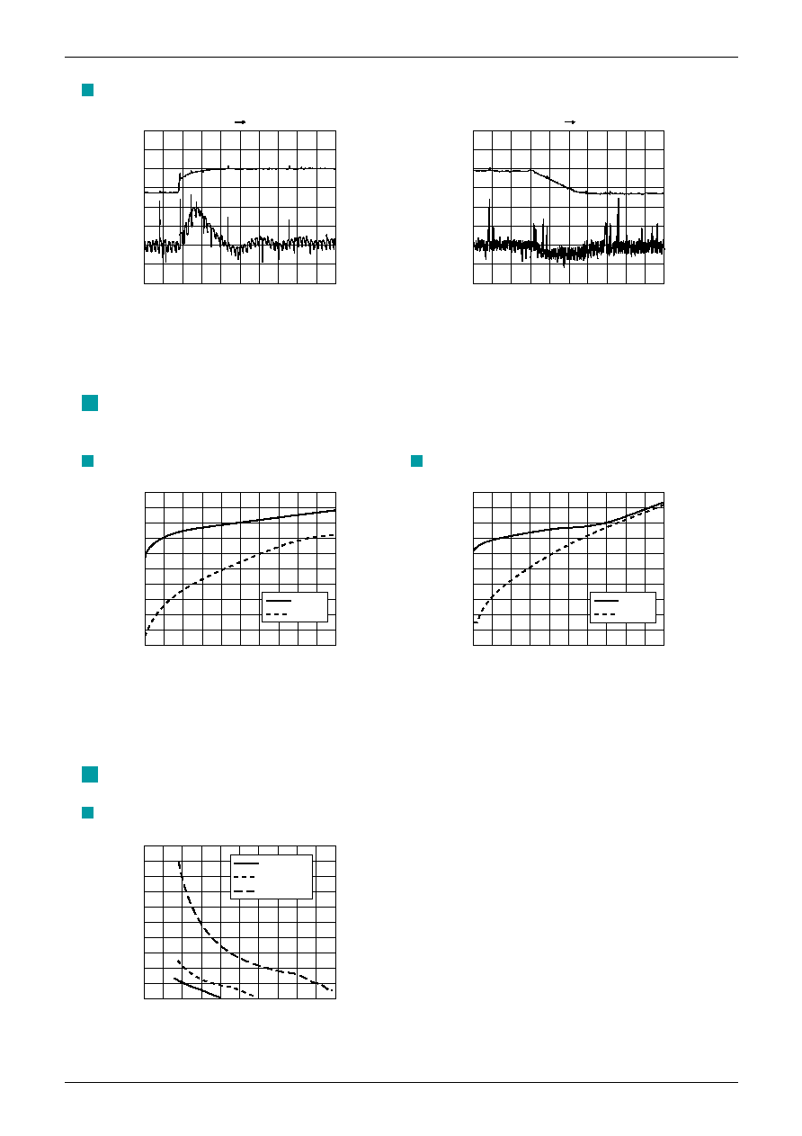
V
IN
: 1.8V 2.4V, I
OUT
=50mA
t (100
µ
s/div)
Input
Voltage
V
IN
(500mV/div)
Output
Voltage
V
OUT
(50mV/div)
V
IN:
2.4V 1.8V, I
OUT
=50mA
t (200
µ
s/div)
Input
Voltage
V
IN
(500mV/div)
Output
Voltage
V
OUT
(50mV/div)
4. Line regulation
0.0
0.1
0.2
0.3
0.4
0.5
0.6
0.7
0.8
0.9
1.0
0
10
9
8
7
6
5
4
3
2
1
Output Current I
OUT
(mA)
Input Voltage V
IN
(V)
VST1
VHLD
0.0
0.1
0.2
0.3
0.4
0.5
0.6
0.7
0.8
0.9
Output Current I
OUT
(mA)
1.0
0
10
9
8
7
6
5
4
3
2
1
Input Voltage V
IN
(V)
VST1
VHLD
MM3005EN
Output current vs starting output voltage and holding output voltage
dependence characteristic
Input voltage vs supply current dependency charavteristic
MM3005H
0
50
100
150
200
250
300
350
400
450
Input Voltage V
IN
(V)
500
0.0
5.0
4.5
4.0
3.5
3.0
2.5
2.0
1.5
1.0
0.5
Input Current I
IN
(
µ
A)
V
OUT
=2V
V
OUT
=3V
V
OUT
=5V
MM3005
Note: these are typical characteristics.

MITSUMI
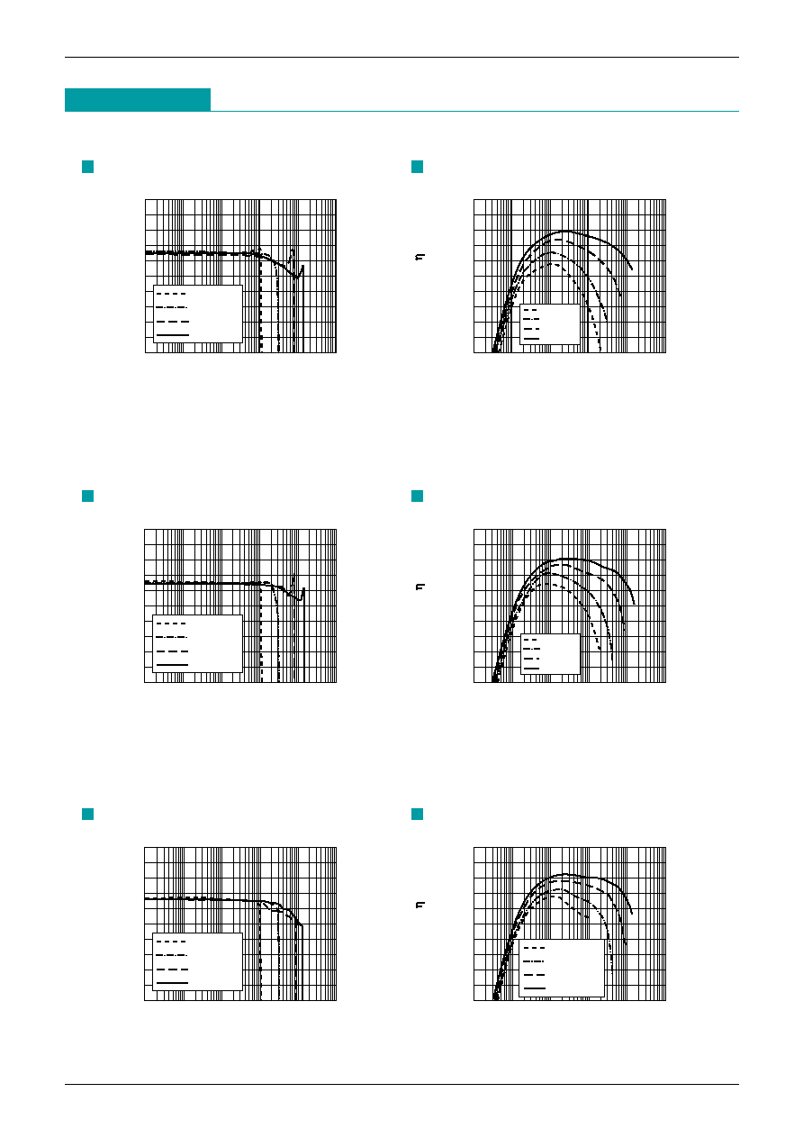
CMOS Switching Regulator (PWM controlled) MM3005~MM3010
2.95
2.96
2.97
2.98
2.99
3.00
3.01
3.02
3.03
3.04
3.05
0.01
0.1
1
10
100
1000
Output Current I
OUT
(mA)
Output Voltage V
OUT
(V)
V
IN
=0.9V
V
IN
=1.2V
V
IN
=1.8V
V
IN
=2.4V
50
55
60
65
70
75
80
85
90
95
100
0.01
0.1
1
10
100
1000
Output Current I
OUT
(
∞
C)
Efficiency (%)
V
IN
=0.9V
V
IN
=1.2V
V
IN
=1.8V
V
IN
=2.4V
Output current vs output voltage
(1) MM3005EN (C5-K3L : 47µH)
(2) MM3005EN (C5-K3L : 100µH)
(3) MM3005EN (C5-K3L : 150µH)
Output current vs efficiency
2.95
2.96
2.97
2.98
2.99
3.00
3.01
3.02
3.03
3.04
3.05
0.01
0.1
1
10
100
1000
Output Current I
OUT
(mA)
Output Voltage V
OUT
(V)
V
IN
=0.9V
V
IN
=1.2V
V
IN
=1.8V
V
IN
=2.4V
50
55
60
65
70
75
80
85
90
95
100
0.01
0.1
1
10
100
1000
Output Current I
OUT
(
∞
C)
Efficiency (%)
V
IN
=0.9V
V
IN
=1.2V
V
IN
=1.8V
V
IN
=2.4V
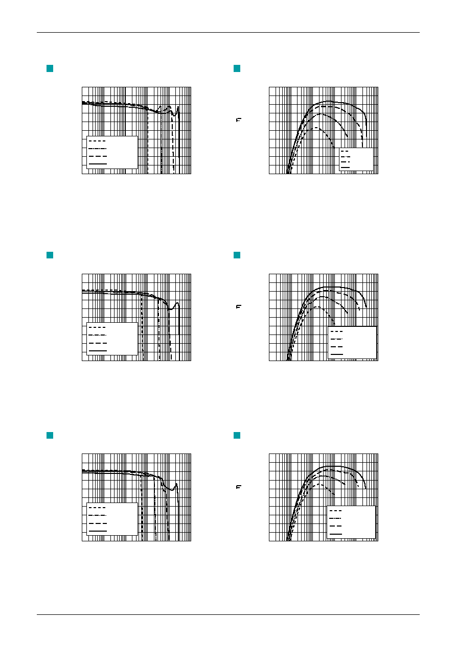
Output current vs output voltage
Output current vs efficiency
2.95
2.96
2.97
2.98
2.99
3.00
3.01
3.02
3.03
3.04
3.05
0.01
0.1
1
10
100
1000
Output Current I
OUT
(mA)
Output Voltage V
OUT
(V)
V
IN
=0.9V
V
IN
=1.2V
V
IN
=1.8V
V
IN
=2.4V
Output current vs output voltage
50
55
60
65
70
75
80
85
90
95
100
0.01
0.1
1
10
100
1000
Output Current I
OUT
(
∞
C)
Efficiency (%)
V
IN
=0.9V
V
IN
=1.2V
V
IN
=1.8V
V
IN
=2.4V
Output current vs efficiency
Reference Data
Note: these are typical characteristics.

MITSUMI
CMOS Switching Regulator (PWM controlled) MM3005~MM3010
4.90
4.92
4.94
4.96
4.98
5.00
5.02
5.04
5.06
5.08
5.10
0.01
0.1
1
10
100
1000
Output Current I
OUT
(mA)
Output Voltage V
OUT
(V)
V
IN
=0.9V
V
IN
=1.8V
V
IN
=3.0V
V
IN
=4.0V
50
55
60
65
70
75
80
85
90
95
100
0.01
0.1
1
10
100
1000
Output Current I
OUT
(mA)
Efficiency (%)
V
IN
=0.9V
V
IN
=1.8V
V
IN
=3.0V
V
IN
=4.0V
Output current vs output voltage
(4) MM3005HN (C5-K3L : 47µH)
(5) MM3005HN (C5-K3L : 100µH)
(6) MM3005HN (C5-K3L : 150µH)
Output current vs efficiency
4.90
4.92
4.94
4.96
4.98
5.00
5.02
5.04
5.06
5.08
5.10
0.01
0.1
1
10
100
1000
Output Current I
OUT
(mA)
Output Voltage V
OUT
(V)
V
IN
=0.9V
V
IN
=1.8V
V
IN
=3.0V
V
IN
=4.0V
55
50
60
65
70
75
80
85
90
95
100
0.01
0.1
1
10
100
1000
Output Current I
OUT
(mA)
Efficiency (%)
V
IN
=0.9V
V
IN
=1.8V
V
IN
=3.0V
V
IN
=4.0V
Output current vs output voltage
Output current vs efficiency
4.90
4.92
4.94
4.96
4.98
5.00
5.02
5.04
5.06
5.08
Output Current I
OUT
(mA)
5.10
0.01
0.1
1
10
100
1000
Output Voltage V
OUT
(V)
V
IN
=0.9V
V
IN
=1.8V
V
IN
=3.0V
V
IN
=4.0V
Output current vs output voltage
50
55
60
65
70
75
80
85
90
95
100
0.01
0.1
1
10
100
1000
Output Current I
OUT
(mA)
Efficiency (%)
V
IN
=0.9V
V
IN
=1.8V
V
IN
=3.0V
V
IN
=4.0V
Output current vs efficiency
Note: these are typical characteristics.

MITSUMI
CMOS Switching Regulator (PWM controlled) MM3005~MM3010
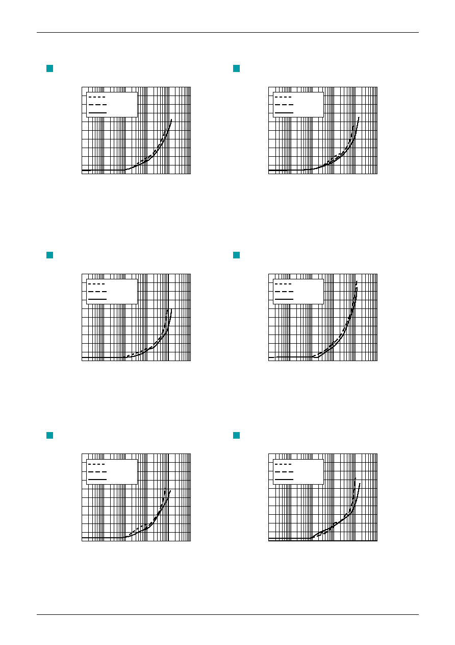
0
10
20
30
40
50
60
70
80
90
100
0.01
0.1
1
10
100
1000
Output Current I
OUT
(mA)
Ripple Voltage Vr (mV)
V
IN
=0.9V
V
IN
=1.8V
V
IN
=2.4V
Output current vs ripple voltage
(7) MM3005EN (C5-K3L : 47µH, C
OUT
: 33µF)
(8) MM3005EN (C5-K3L : 100µH, C
OUT
: 33µF)
(9) MM3005EN (C5-K3L : 150µH, C
OUT
: 33µF)
0
10
20
30
40
50
60
70
80
90
100
0.01
0.1
1
10
100
1000
Output Current I
OUT
(mA)
Ripple Voltage Vr (mV)
V
IN
=0.9V
V
IN
=1.8V
V
IN
=2.4V
Output current vs ripple voltage
0
10
20
30
40
50
60
70
80
90
Output Current I
OUT
(mA)
100
0.01
0.1
1
10
100
1000
Ripple Voltage Vr (mV)
V
IN
=0.9V
V
IN
=1.8V
V
IN
=2.4V
Output current vs ripple voltage
Note: these are typical characteristics.
0
10
20
30
40
50
60
70
80
90
100
0.01
0.1
1
10
100
1000
Output Current I
OUT
(mA)
Ripple Voltage Vr (mV)
V
IN
=0.9V
V
IN
=3.0V
V
IN
=4.0V
Output current vs ripple voltage
(10) MM3005HN (C5-K3L : 47µH, C
OUT
: 33µF)
(11) MM3005HN (C5-K3L : 100µH, C
OUT
: 33µF) (12) MM3005HN (C5-K3L : 150µH, C
OUT
: 33µF)
0
10
20
30
40
50
60
70
80
90
100
0.01
0.1
1
10
100
1000
Output Current I
OUT
(mA)
Ripple Voltage Vr (mV)
V
IN
=0.9V
V
IN
=3.0V
V
IN
=4.0V
Output current vs ripple voltage
0
10
20
30
40
50
60
70
80
90
100
0.01
0.1
1
10
100
1000
Output Current I
OUT
(mA)
Ripple Voltage Vr (mV)
V
IN
=0.9V
V
IN
=3.0V
V
IN
=4.0V
Output current vs ripple voltage
