 | –≠–ª–µ–∫—Ç—Ä–æ–Ω–Ω—ã–π –∫–æ–º–ø–æ–Ω–µ–Ω—Ç: MM3055RU | –°–∫–∞—á–∞—Ç—å:  PDF PDF  ZIP ZIP |

MITSUMI
Regulator with ON/OFF MM3051 ~MM3055 U
Regulator with ON/OFF
Monolithic IC MM3051 ~MM3055 U
Outline
Outline
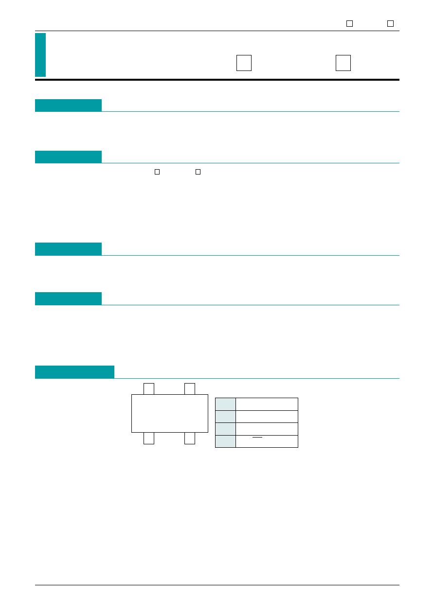
This IC is a low current consumption (1.5µA typ.), ultra-small CMOS regulator with ON/OFF control function.
The ON/OFF control pin logic for MM3051H ~ MM3055F and MM3051T ~ MM3055R is reversed.
Features
1. I/O voltage difference (MM3054 ~ MM3055 ) 25mV typ. (I
O
=1mA)
2. Current consumption
1.5µA typ. (V
IN
=V
O
+2V)
3. Output current
80mA min. (V
IN
-V
OUT
=2V)
4. Output voltage rank
1.7~5.5V (0.1V step)
5. Output ON/OFF control function
High: ON, Low: OFF (MM3051H~MM3055F)
High: OFF, Low: ON (MM3051T~MM3055R)
SC-82ABA
SC-82ABB
Applications
Applications
Package
1. Portable equipment
2. Cellular telephone, PHS
3. Cordless telephone
4. Other battery-powered portable equipment
Pin Assignment
1
2
4
3
SC-82ABA
SC-82ABB
(TOP VIEW)
1
GND
2
V
DD
3
V
OUT
4
CE or CE
The ON/OFF control pin logic for MM3051H ~ MM3055F and MM3051T ~ MM3055R is reversed

MITSUMI
Regulator with ON/OFF MM3051 ~MM3055 U
Equivalent Circuit Diagram
V
CE
4
10k
V
DD
2
GND
Current
Limit
REF
1
OUT
V
3
4M
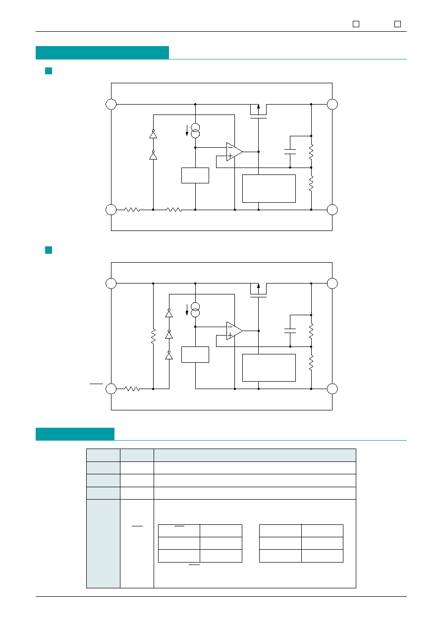
MM3051H ~ MM3055FU
V
CE
4
10k
V
DD
2
GND
Current
Limit
REF
1
OUT
V
3
4M
Pin Description
Pin No.
Pin name
Function
1
GND
GND Pin
2
V
DD
Voltage supply pin
3
V
OUT
Regulator output voltage pin
Output voltage ON/OFF-Control pin
MM3051T~MM3055R
CE
4
or
CE
Connect CE pin with GND
pin, when it is not used.
CE
Output
L
ON
H
OFF
CE
Output
L
OFF
H
ON
MM3051T ~ MM3055RU
MM3051H~MM3055F
Connect the CE pin to V
DD
when not using it.

MITSUMI
Regulator with ON/OFF MM3051 ~MM3055 U
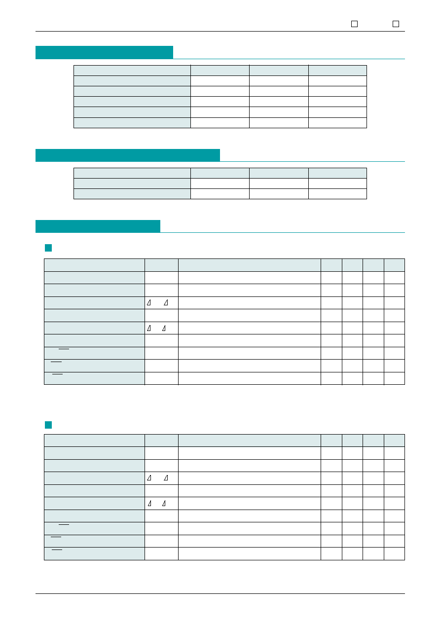
Absolute Maximum Ratings
(Except where noted therwise, Ta=25∞C)
Item
Symbol
Ratings
Units
Storage temperature
T
STG
-40~+125
∞C
Operating temperature
T
OPR
-30~+85
∞C
Supply voltage
V
DD
-0.3~+9
V
Output current
I
OUT
150
mA
Allowable loss
Pd
150 (Alone)
mW
Recommended Operating Conditions
(Except where noted therwise, Ta=25∞C)
Item
Symbol
Ratings
Units
Operating temperature
T
OP
-30~+85
∞C
Supply voltage
V
OP
V
OUT
+0.3~8
V
Electrical Characteristics
(Except where noted therwise, Ta=25∞C, V
CE
=V
IN
)
Item
Symbol
Measurement conditions
Min. Typ. Max. Units
Supply current
I
SS
V
IN
=V
OUT
+2.0V, Excluding CE Pin Current (I
CE
)
1.5
3.0
µA
Supply current (OFF)
Istandby
V
IN
=V
OUT
+2.0V, V
CE
=V
IN
0.1
1.0
µA
Line regulation
V
OUT
/ V
IN
I
OUT
=1mA, V
OUT
+0.5V <
= V
IN
<
= 8V
0
0.05
0.20
%/V
Input voltage
V
IN
8.0
V
Vo temperature coefficient
V
OUT
/ Vopt
I
OUT
=10mA -30∞C <
= T
OPT
<
= 85∞C
±100
ppm/∞C
Output short-circuit current
Ilim
V
IN
=V
OUT
+2.0V, V
OUT
=0V
60
mA
CE pull down resistance
R
PD
V
IN
=V
OUT
+2.0V
1.5
4.0
12.0
M
CE high threshold voltage
V
CEH
V
IN
=V
OUT
+2.0V
1.5
V
CE low threshold voltage
V
CEL
V
IN
=V
OUT
+2.0V
0.25
V
Note:
V
OUT
is the output voltage typ. value in the specifications.
Make sure that output current does not exceed loss tolerance.
Item
Symbol
Measurement conditions
Min. Typ. Max. Units
Supply current
I
SS
V
IN
=V
OUT
+2.0V, Excluding CE Pin Current (I
CE
)
1.5
3.0
µA
Supply current (OFF)
Istandby
V
IN
=V
OUT
+2.0V, V
CE
=V
IN
0.1
1.0
µA
Line regulation
V
OUT
/ V
IN
I
OUT
=1mA, V
OUT
+0.5V <
= V
IN
<
= 8V
0
0.05
0.20
%/V
Input voltage
V
IN
8.0
V
Vo temperature coefficient
V
OUT
/ Vopt
I
OUT
=10mA -30∞C <
= T
OPT
<
= 85∞C
±100
ppm/∞C
Output short-circuit current
Ilim
V
IN
=V
OUT
+2.0V, V
OUT
=0V
60
mA
CE pull up resistance
R
PU
V
IN
=V
OUT
+2.0V
1.5
4.0
12.0
M
CE high threshold voltage
V
CEH
V
IN
=V
OUT
+2.0V
1.5
V
CE low threshold voltage
V
CEL
V
IN
=V
OUT
+2.0V
0.25
V
Note:
V
OUT
is the output voltage typ. value in the specifications.
Make sure that output current does not exceed loss tolerance.
MM3051H ~ MM3055FU
MM3051T ~ MM3055RU
(Except where noted therwise, Ta=25∞C, V
CE
=GND)

MITSUMI
Regulator with ON/OFF MM3051 ~MM3055 U
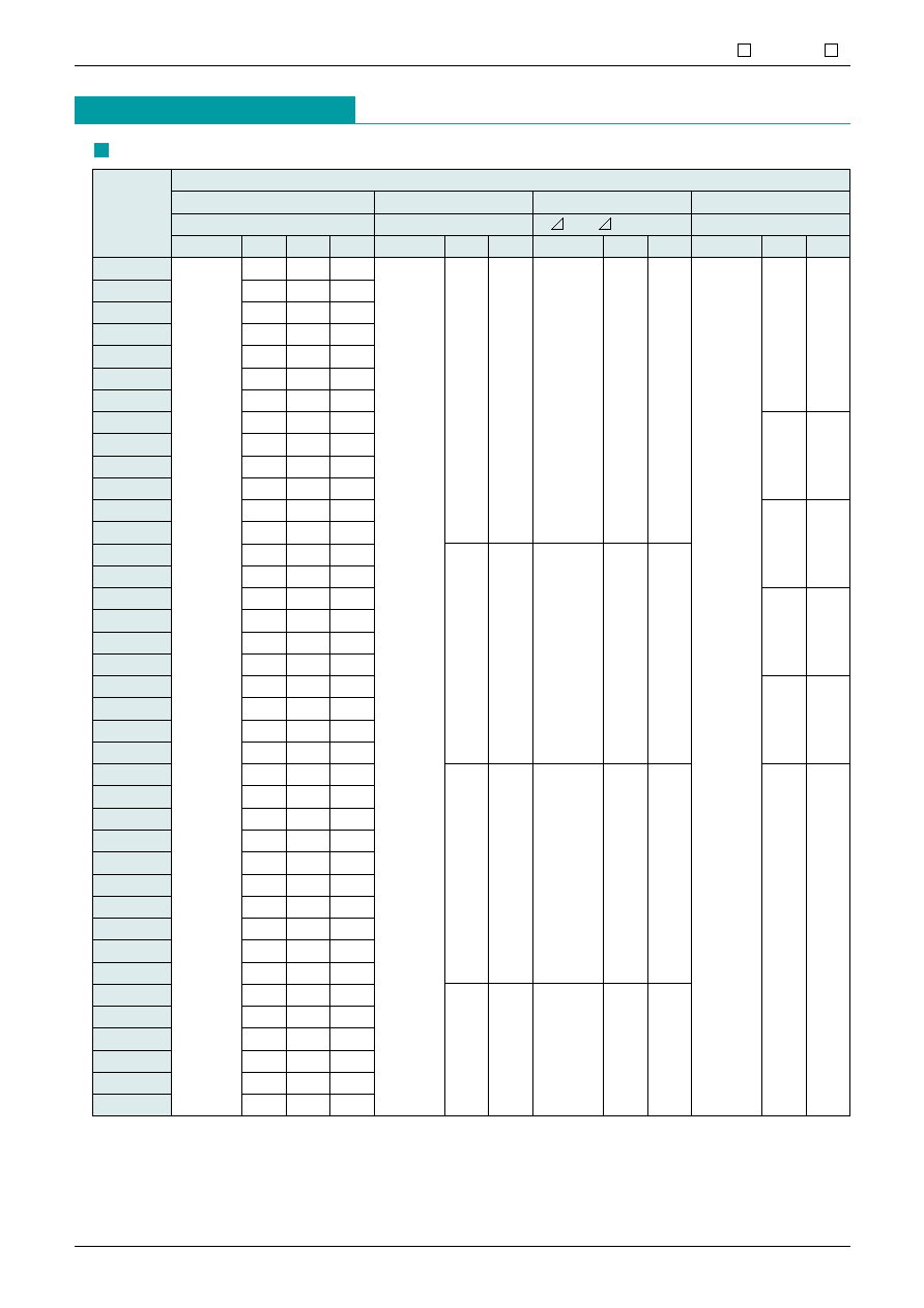
Electrical Characteristics 2
High Active (Except where noted therwise, Ta=25∞C, V
IN
=V
CE
)
Item
Product
Output voltage
Output current
Load regulation
Input-Output differential voltage
name
V
OUT
(V)
I
OUT
(mA)
V
OUT
/ I
OUT
(mV)
V
DIF
(mV)
Test Condisions Min. Typ. Max. Test condisions Min. Typ. Test condisions Typ. Max. Test condisions Typ. Max.
MM3051H
1.666 1.700 1.734
MM3051J
1.764 1.800 1.836
MM3051K
1.862 1.900 1.938
MM3052A
1.960 2.000 2.040
MM3052B
2.058 2.100 2.142
MM3052C
2.156 2.200 2.244
MM3052D
2.254 2.300 2.346
MM3052E
2.352 2.400 2.448
MM3052F
2.450 2.500 2.550
MM3052G
2.548 2.600 2.652
MM3052H
2.646 2.700 2.754
MM3052J
2.744 2.800 2.856
MM3052K
2.842 2.900 2.958
MM3053A
2.940 3.000 3.060
MM3053B
3.038 3.100 3.162
MM3053C
3.136 3.200 3.264
MM3053D
3.234 3.300 3.366
MM3053E
3.332 3.400 3.468
MM3053F
3.430 3.500 3.570
MM3053G
3.528 3.600 3.672
MM3053H
3.626 3.700 3.774
MM3053J
3.724 3.800 3.876
MM3053K
3.822 3.900 3.978
MM3054A
3.920 4.000 4.080
MM3054B
4.018 4.100 4.182
MM3054C
4.116 4.200 4.284
MM3054D
4.214 4.300 4.386
MM3054E
4.312 4.400 4.488
MM3054F
4.410 4.500 4.590
MM3054G
4.508 4.600 4.692
MM3054H
4.606 4.700 4.794
MM3054J
4.704 4.800 4.896
MM3054K
4.802 4.900 4.998
MM3055A
4.900 5.000 5.100
MM3055B
4.998 5.100 5.202
MM3055C
5.096 5.200 5.304
MM3055D
5.194 5.300 5.406
MM3055E
5.292 5.400 5.508
MM3055F
5.390 5.500 5.610
V
IN
-V
OUT
=2.0V
10µA <
=
I
OUT
<
=
10mA
V
IN
-V
OUT
=2.0V
V
IN
-V
OUT
=2.0V
1mA <
=
I
OUT
<
=
35mA
30
35
V
IN
-V
OUT
=2.0V
1mA <
=
I
OUT
<
=
50mA
V
IN
-V
OUT
=2.0V
1mA <
=
I
OUT
<
=
65mA
50
65
80
I
OUT
=1mA
60
90
50
75
40
60
35
55
30
45
25
40
V
IN
-V
OUT
=2.0V
1mA <
=
I
OUT
<
=
80mA
45
40
60
50
70
60
90
MM3051H ~ MM3055FU

MITSUMI
Regulator with ON/OFF MM3051 ~MM3055 U
Item
Product
Output voltage
Output current
Load regulation
Input-Output differential voltage
name
V
OUT
(V)
I
OUT
(mA)
V
OUT
/ I
OUT
(mV)
V
DIF
(mV)
Test condisions Min. Typ. Max. Test condisions Min. Typ. Test condisions Typ. Max. Test condisions Typ. Max.
MM3051T
1.666 1.700 1.734
MM3051U
1.764 1.800 1.836
MM3051V
1.862 1.900 1.938
MM3052L
1.960 2.000 2.040
MM3052M
2.058 2.100 2.142
MM3052N
2.156 2.200 2.244
MM3052P
2.254 2.300 2.346
MM3052Q
2.352 2.400 2.448
MM3052R
2.450 2.500 2.550
MM3052S
2.548 2.600 2.652
MM3052T
2.646 2.700 2.754
MM3052U
2.744 2.800 2.856
MM3052V
2.842 2.900 2.958
MM3053L
2.940 3.000 3.060
MM3053M
3.038 3.100 3.162
MM3053N
3.136 3.200 3.264
MM3053P
3.234 3.300 3.366
MM3053Q
3.332 3.400 3.468
MM3053R
3.430 3.500 3.570
MM3053S
3.528 3.600 3.672
MM3053T
3.626 3.700 3.774
MM3053U
3.724 3.800 3.876
MM3053V
3.822 3.900 3.978
MM3054L
3.920 4.000 4.080
MM3054M
4.018 4.100 4.182
MM3054N
4.116 4.200 4.284
MM3054P
4.214 4.300 4.386
MM3054Q
4.312 4.400 4.488
MM3054R
4.410 4.500 4.590
MM3054S
4.508 4.600 4.692
MM3054T
4.606 4.700 4.794
MM3054U
4.704 4.800 4.896
MM3054V
4.802 4.900 4.998
MM3055L
4.900 5.000 5.100
MM3055M
4.998 5.100 5.202
MM3055N
5.096 5.200 5.304
MM3055P
5.194 5.300 5.406
MM3055Q
5.292 5.400 5.508
MM3055R
5.390 5.500 5.610
V
IN
-V
OUT
=2.0V
10µA <
=
I
OUT
<
=
10mA
V
IN
-V
OUT
=2.0V
V
IN
-V
OUT
=2.0V
1mA <
=
I
OUT
<
=
35mA
30
35
V
IN
-V
OUT
=2.0V
1mA <
=
I
OUT
<
=
50mA
V
IN
-V
OUT
=2.0V
1mA <
=
I
OUT
<
=
65mA
50
65
80
I
OUT
=1mA
60
90
50
75
40
60
35
55
30
45
25
40
V
IN
-V
OUT
=2.0V
1mA <
=
I
OUT
<
=
80mA
45
40
60
50
70
60
90
MM3051T ~ MM3055RU
Electrical Characteristics 3
Low Active (Except where noted therwise, Ta=25∞C, V
CE
=GND)

MITSUMI
Regulator with ON/OFF MM3051 ~MM3055 U
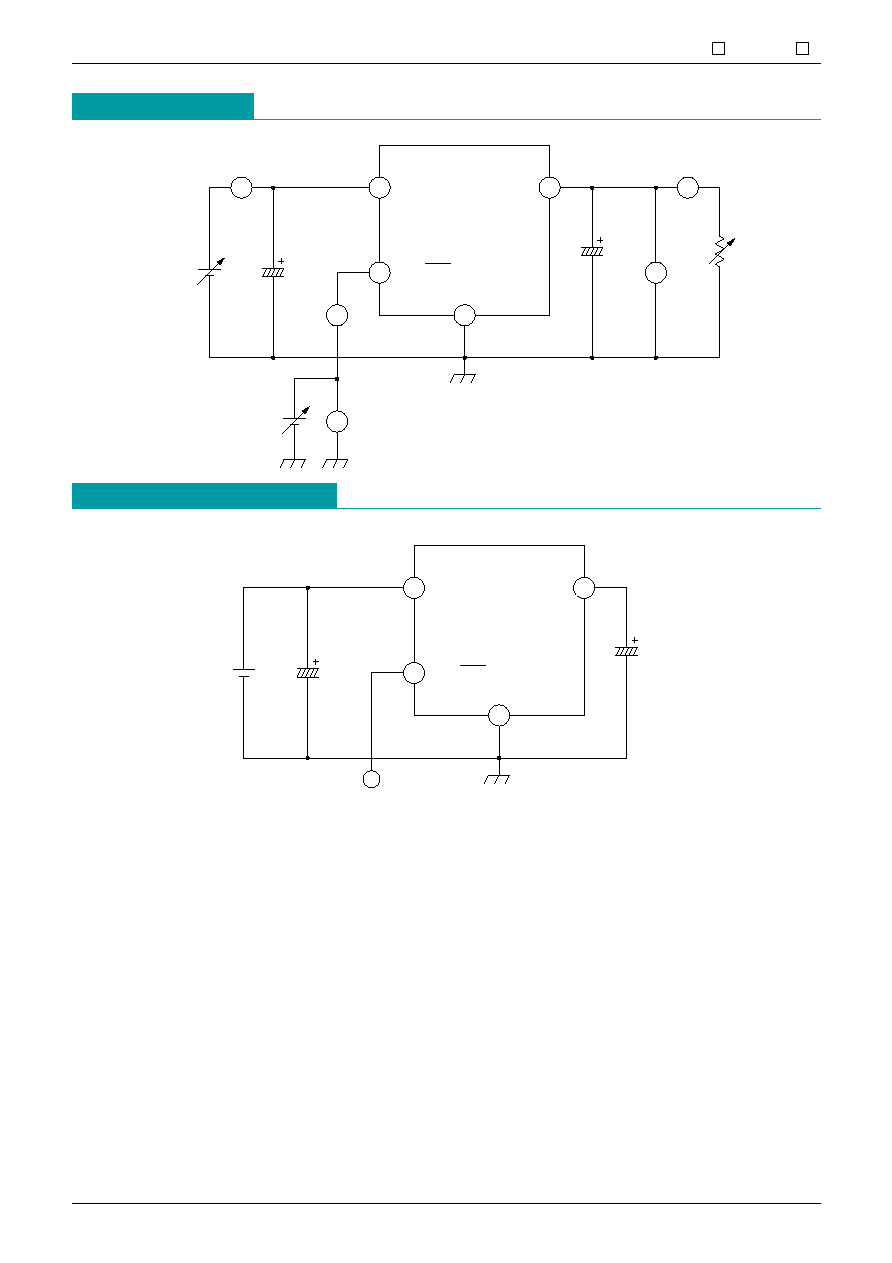
Measuring Circuit
A
CE
V
V
C1
IN
V
A
1
C1,C2=1
µ
F (AL-Electlytic)
MM305X
CE,CE
4
2
V
DD
GND
OUT
V
3
V
C2
A
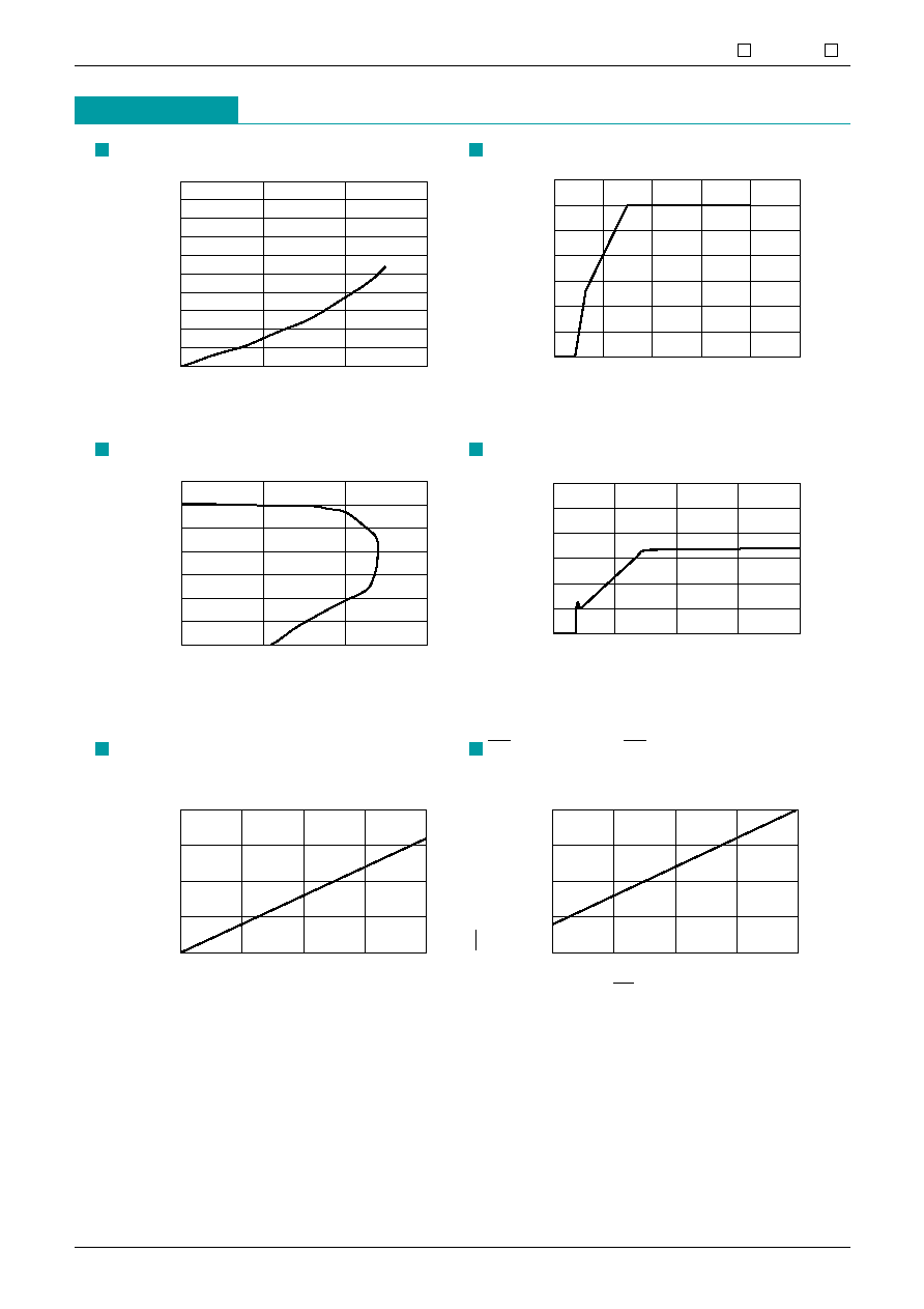
Typical Application Circuit
ON/OFF
C1
IN
V
1
C1,C2=1
µ
F (AL-Electlytic)
MM305X
CE,CE
4
2
V
DD
GND
OUT
V
3
C2
note: This regulator is not internally compensated and thus require an external output-capacitor (C
OUT
) for
stability.

MITSUMI
Regulator with ON/OFF MM3051 ~MM3055 U
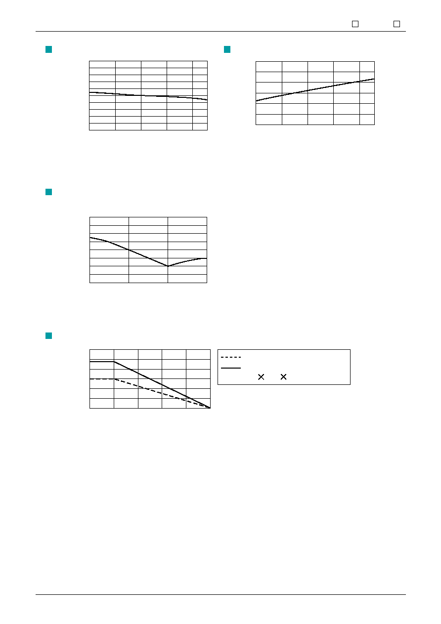
Characteristics
(3.0V product except where noted therwise, Ta=25∞C)
0.0
60
40
20
0
0.4
1.6
1.2
0.8
0.2
1.4
1.0
0.6
1.8
2.0
0.0
6
2
10
8
4
0
2.0
1.5
1.0
0.5
2.5
3.5
3.0
I
OUT
=1mA
0.0
50
150
100
0
Output Current (mA)
2.0
1.5
1.0
0.5
2.5
3.5
V
IN
=5V
3.0
Output Voltage (V)
0.0
8
4
6
2
0
Input Voltage (V)
2.0
1.5
1.0
0.5
2.5
3.0
Supply Current (
µ
A)
0.0
6
2
8
4
0
CE Pin Voltage (V)
1.5
1.0
0.5
2.0
V
IN
=8V
CE Pin Current (
µ
A)
-2.0
6
2
8
4
0
CE Pin Voltage (V)
-0.5
-1.0
-1.5
0.0
V
IN
=8V
CE Pin Current (
µ
A)
Input-Output Differential Voltage
Line Regulation
Load Regulation
Supply Current
CE Pin Current VS CE Pin Voltage High Active
CE Pin Current VS CE Pin Voltage Low Active

MITSUMI
Regulator with ON/OFF MM3051 ~MM3055 U
Temperature (
∞
C)
2.90
85
70
-5
45
20
-30
3.06
3.04
3.02
3.00
2.98
2.94
2.92
3.10
2.96
3.08
Output Voltage (V)
Temperature (
∞
C)
70
45
85
20
-5
-30
Input Current (
µ
A)
0.0
0.5
1.0
1.5
2.0
2.5
3.0
Temperature (
∞
C)
0
125
50
100
25
75
0
100
300
200
250
50
150
Alone
Allowable Loss (mW)
On Board (Glass Epoxy Resin)
100 100 1.6mm
0
100
1
10
0.1
Frequency (kHz)
50
40
30
20
10
60
80
70
Ripple Rejection (dB)
V
IN
=5V DC, 0.5V
P-P
AC
I
OUT
=10mA
Output Voltage VS Temperature
Input Current VS Temperature
Allowable Loss
Ripple Rejection
