MITSUMI
System Reset PST591~595
System Reset
Monolithic IC PST591~595 Series
Outline
These ICs function in a variety of CPU systems and other logic systems, to detect power supply voltage and
reset the system accurately when power is turned on or interrupted, and has a built-in fixed delay time
generating circuit. This series has been represented in the past by PST574/PST575, but these new low reset
type system reset ICs expand the delay time series with a counter timer using an analog/digital hybrid circuit.
Features
1. Fixed delay time setting by counter timer
Excellent delay time temperature characteristics
±800ppm/
∞
C
2. Low operating limit voltage
0.65V typ.
3. Hysteresis voltage provided in detection voltage
50mV typ.
4. Current consumption for no-load
I
CCL
=300µA typ. I
CCH
=200µA typ.
5. 5 delay time products available
PST591
50ms
PST594 400ms
PST592 100ms
PST595 800ms
PST593 200ms
6. Each product has 9 detection voltage ranks.
C : 4.5V typ.
H : 3.1V typ.
D : 4.2V typ.
I : 2.9V typ.
E : 3.9V typ.
J : 2.7V typ.
F : 3.6V typ.
K : 2.5V typ.
G : 3.3V typ.
Package
MMP-4A (PST59 M)
TO-92A (PST59 )
*
contains detection voltage rank.
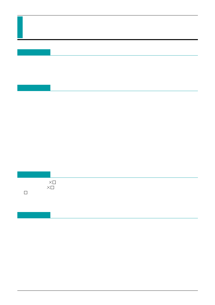
(MMP-4A has a manual reset pin, which should be set at GND or NC during normal operation.)
Applications
1. Reset circuits in microcomputers, CPUs and MPUs
2. Logic circuit reset circuits.
3. Battery voltage check circuits.
4. Back-up power supply switching circuits.
5. Level detection circuits.
6. Mechanical reset circuits

MITSUMI
System Reset PST591~595
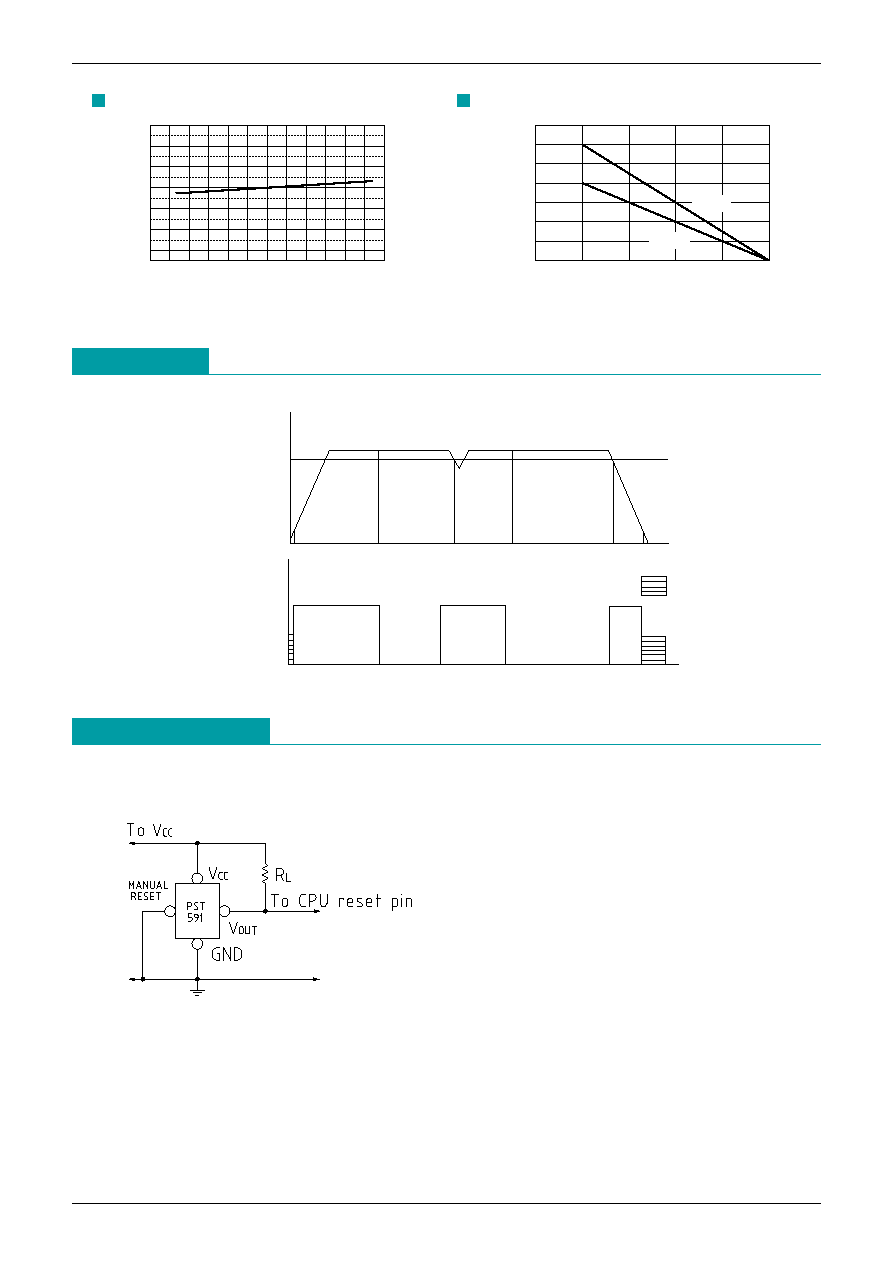
Measuring Circuit
[1]
[2]
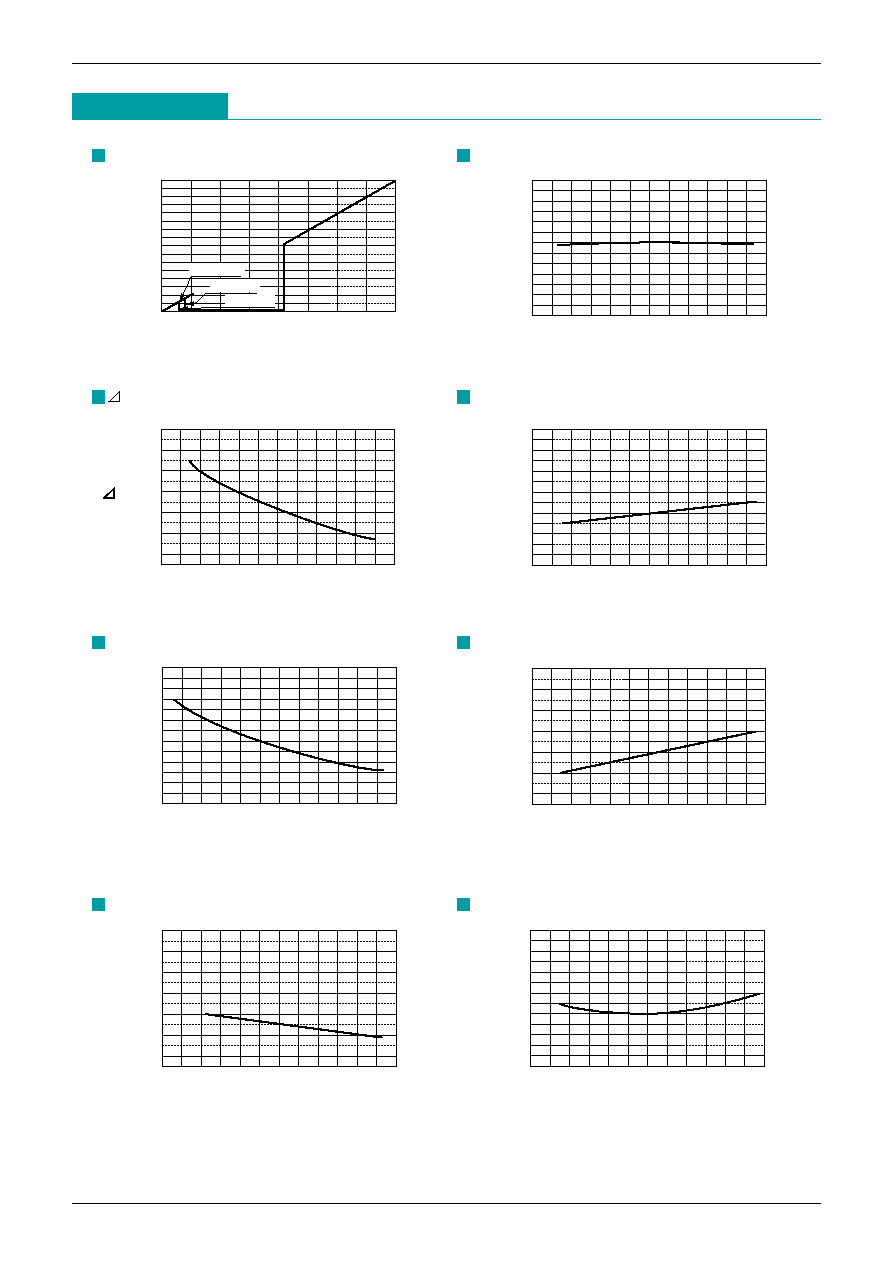
Electrical Characteristics
(Ta=25
∞
C) (Except where noted otherwise, resistance unit is
)
*
1 tpLH : V
CC
= (V
S
typ.-0.4V) (V
S
typ.+0.4V), tpHL : V
CC
= (V
S
typ.+0.4V) (V
S
typ.-0.4V)
*
2 V
CC
=V
S
min.-0.15V
Note 3: V
OUT
pin is low when manual reset pin is high.
V
OUT
pin is high when manual reset pin is low.
Note: Input model is an example for PST591C.
Item
Symbol Measuring circuit
Measurement conditions
Min. Typ. Max. Unit
C
4.3
4.5
4.7
D
4.0
4.2
4.4
E
3.7
3.9
4.1
R
L
=470
F
3.4
3.6
3.8
Detection voltage
V
S
1
V
OL
<
= 0.4V
G
3.1
3.3
3.5
V
V
CC
=H L
H
2.9
3.1
3.3
I
2.75 2.90 3.05
J
2.55 2.70 2.85
K
2.35 2.50 2.65
Hysteresis voltage
V
S
1
R
L
=470, V
CC
=L H L
30
50
100
mV
Detection voltage
temperature coefficient
V
S
/ T
1
R
L
=470, Ta=-20
∞
C~+75
∞
C
±0.01
%/
∞
C
Low-level output voltage
V
OL
1
V
CC
=Vs min.-0.05V, R
L
=470
0.1
0.4
V
Output leakage current
I
OH
1
V
CC
=10V
±0.1
µA
Circuit current while on
I
CCL
1
V
CC
=Vs min.-0.05V, R
L
=
300
600
µA
Circuit current while off
I
CCH
1
V
CC
=Vs typ./0.85V, R
L
=
200
350
µA
PST591
30
50
75
R
L
=4.7k
PST592
60
100
150
"H" transport delay time
t
PLH
2
C
L
=100PF
*
1
PST593
120
200
300
ms
PST594
240
400
600
PST595
480
800 1200
"L" transport delay time
t
PHL
2
R
L
=4.7k, C
L
=100PF
*
1
10
µs
Operating power supply voltage
V
OPL
1
R
L
=4.7k, V
OL
<
= 0.4V
0.65 0.85
V
Output current while on 1
I
OL
1
1
V
CC
=V
S
min.-0.05V, R
L
=0
8
mA
Output current while on 2
I
OL
2
1
Ta=-20
∞
C~+75
∞
C, R
L
=0
*
2
6
mA
Manual
Input high voltage
V
RESH
2.0
V
reset
Input high current
V
RESH
V
RES
=2V
80
µA
pin
Input low voltage
V
RESL
0.8
V