
MOSA ELECTRONICS
MS6313
Stereo Audio DAC
-
1
-
www.mosanalog.com.tw
FEATURES
Excellent Power Supply Rejection Ratio(PSRR) Easy application :
Voltage Output Operation range: 2.7V~5.5V
Space saving package(SOP8) Output and bias current are proportional to supply voltage
Low power consumption integrated current-to-voltage converter
Low total harmonic distortion
Wide dynamic range(16-bit resolution)
No zero crossing distortion
Wide operating temperature range(-40 to 85)
Internal bias current ensures maximum dynamic range
Fast setting time permits 2*, 4*, and 8* oversampling(serial input) or double speed operation at 4* oversampling
Compatible with most of the Japanese input formats; time multiplexed, two's complement, TTL
The full scale output voltage can be mask optioned
Cost efficient
APPLICATIONS
VCD Player, DVD Player, CD-ROM, DVD-ROM, CD-RW, DVD-RW, Motherboard.
MP3, PDA, Portable Digital Audio.
DESCRIPTION
The MS6313 is a 16-bit voltage-output Digital-to-Analog Converter(DAC). The MS6313 is with excellent Power
Supply Rejection Ratio(PSRR). It is fabricated in a 0.8
µ
m CMOS process and features extremely low power dissipation,
small package size and easy application. The accuracy of the matched coarse current sources, combined with the unique
symmetrical decoding method, preclude zero-crossing distortion and ensures high quality audio reproduction. These
unique features, combined with its exceptional performance, make the MS6313 ideally suited for use in digital audio
equipment. MS6313 is pin and function compatible with the Philips, TDA1311.
PINNING
Symbol Pin
Description
BCK
1
bit clock input
WS
2
word select input
DATA
3
data input
GND
4
ground
V
DD
5
positive supply voltage
V
OL
6
left channel output
Cap
7
Cap
V
OR
8
right channel output
7
6
5
8
2
3
4
1
MS6313
V
OR
Cap
V
OL
V
DD
BCK
WS
DATA
GND
Pin configuration
Pin 7 : Capacitor = 10
µ
F (ripple rejection)
MOSA ELECTRONICS
MS6313
Stereo Audio DAC
-
2
-
www.mosanalog.com.tw
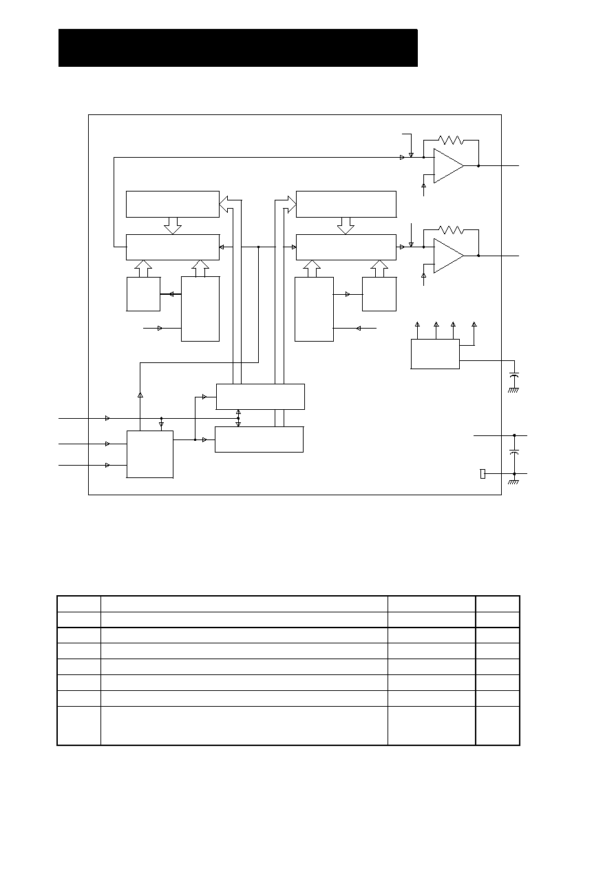
BLOCK DIAGRAM
LEFT OUTPUT LATCH
LEFT BIT SWITCHES
11-BIT
PASSIVE
DIVIDER
32 (5-BIT)
MATCHED
CURRENT
SOURCES
Iref
RIGHT OUTPUT LATCH
RIGHT BIT SWITCHES
32 (5-BIT)
MATCHED
CURRENT
SOURCE
11-BIT
PASSIVE
DIVIDER
Iref
LEFT INPUT LATCH
RIGHT INPUT LATCH
CONTROL
&
TIMING
Vref
Vref
R1
R2
REFERENCE
SOURCE
I
BL
Iref I
BR
I
BL
I
BR
-
+
-
+
1
2
3
BCK
WS
DATA
6
8
V
OUT
left
V
OUT
right
5
V
DD
4
GND
OP1
OP2
100nF
Vref
2K
2K
1uF
7
nc / Cap
10uF
cap
Fig.1 Block diagram.
LIMITING VALUES
Symbol
Parameter Rating
Unit
V
DD
Positive Supply Voltage
6
V
T
STG
Storage Temperature Range
-65 to 150
T
A
Operating Ambient Temperature Range
-40 to 85
T
J
Maximum Junction Temperature
150
T
S
Soldering Temperature, 10 seconds
260
T
ESD
Electrostatic Handling
-2000 to 2000
V
R
THJA
Thermal Resistance from Junction to Ambient in Free Air
SOP8
210
/W

MOSA ELECTRONICS
MS6313
Stereo Audio DAC
-
3
-
www.mosanalog.com.tw
ELECTRICAL CHARACTERISTICS
(Ta=25, V
DD
=5V)
Symbol Parameter
Conditions
Min
Typ
Max
Unit
V
DD
Positive Supply Voltage
2.7 5 5.5 V
I
DD
Operating Current
at code 0000H
-
3.4
6.0
mA
DIGITAL INPUTS (WS, BCK, DATA)
Symbol Parameter
Conditions
Min
Typ
Max
Unit
l
I
IL
l
Input Leakage Current LOW
V
I
=
0.8V -
-
10
µ
A
l
I
IH
l
Input Leakage Current HIGH
V
I
=
2.4V -
-
10
µ
A
f
BCK
Input Clock Frequency
-
-
18.4
MHz
BR
Bit Rate Data Input (Pin 3)
-
-
18.4
Mbits/s
f
WS
Word Select Input (Pin 2)
-
-
384
kHz
t
r
Rise Time
-
-
12
ns
t
f
Fall Time
-
-
12
ns
t
C
r
Bit Clock Cycle Time
54
-
-
ns
t
HB
Bit Clock High Time
15
-
-
ns
t
LB
Bit Clock Low Time
15
-
-
ns
t
SD
Data Set-up Time
12
-
-
ns
t
HD
Data Hold Time to Bit Clock
2
-
-
ns
t
HW
Word Select Hold Time
2
-
-
ns
t
SW
Word Select Set-up Time
12
-
-
ns
ANALOG OUTPUTS (V
OL
,V
OR
)
Symbol Parameter
Conditions
Min
Typ
Max
Unit
Res Resolution
-
- 16 bits
V
FS
Full Scale Output Voltage
V
FS
=0.4V
DD
1.8 2.0 2.2 V
T
CFS
Full Scale Temperature Coefficient
at Analog Outputs ; V
OL
, V
OR
-
±
400 - 10-
16
V
DC
Output
Bias
- 2.5 - V
THD
Total Harmonic Distortion
including noise
-
-68
-63
dB
at 0 dB; note 1
-
0.04
0.07
THD
Total Harmonic Distortion
including noise
-
-30
-24
dB
at -60 dB; note 1
-
3
6
CS Channel
Separation
75 80 - dB
l
d
I
O
l
Unbalance Between Outputs
note 1
-
0.2
0.3
dB
l
t
d
l
Time Delay Between Outputs
-
±
0.2 -
µ
s
S/N Signal-to-Noise
Ratio
a-weighted at code
0000H
86 92 - dB
Note : 1.Measured with 1kHz sinewave generated at sampling rate of 192 kHz.
MOSA ELECTRONICS
MS6313
Stereo Audio DAC
-
4
-
www.mosanalog.com.tw
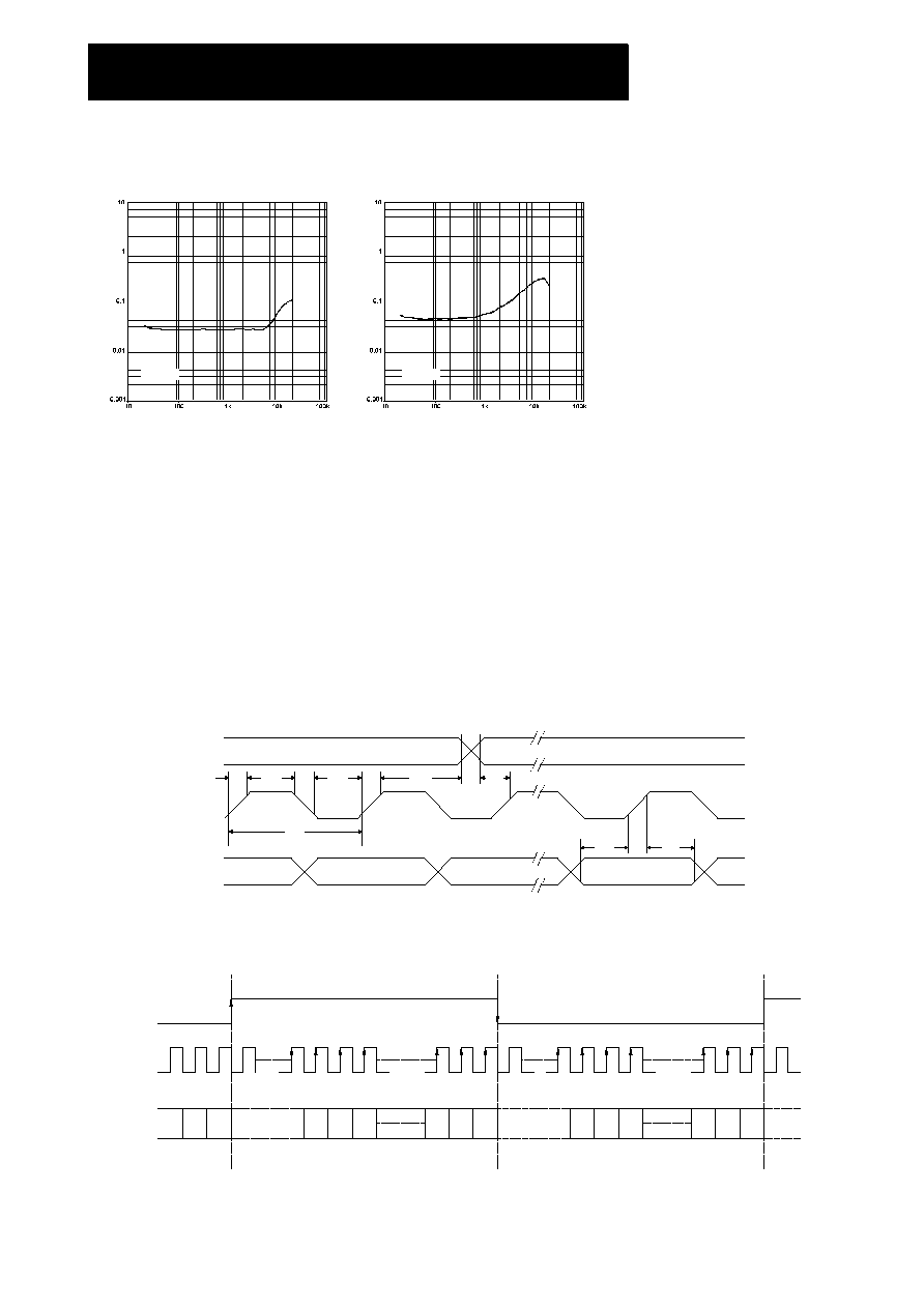
TYPICAL PERFORMANCE CHARACTERISTICS
(Ta=25, R
L
=32
, sampling rate=4fs; unless otherwise specified)
THD+N (%)
FREQUENCY (Hz)
THD+N (%)
FREQUENCY (Hz)
THD+N vs. frequency
THD+N vs. frequency
V
DD
=5V
V
DD
=2.7V
TIMING AND DATA FORMAT
The MS6313 accepts input serial data formats of 16-bit word length. Left and right data words are time
multiplexed. The MSB (bit 1) must always be first. The format of data input is shown in Figs. 2 and 3. With a HIGH
level on the word select input (WS), data is placed in the left input register and with LOW level on the WS input, data is
placed in the right register (Fig. 1). The data in the input registers are simultaneously latched in the output registers
which control the bit switches. Internal bias currents I
BL
and I
BR
are each added to the full scale output current I
FS
in
order to achieve the maximum dynamic range at the outputs of OP1 and OP2(Fig. 1). The reference voltage Vref (Fig. 1)
is approximately 2/3 V
DD
. In this way the maximum dynamic range is achieved over the entire power supply range.
RIGHT
WS
BCK
DATA
LSB
MSB
t
r
t
HB
t
f
t
cr
t
LB
t
HW
t
SW
LEFT
t
SD
t
HD
Fig.2 Timing and input signals.
0
1
2
15
14
13
2
1
0
MSB
LSB
15
14
13
2
1
0
MSB
LSB
RIGHT
LEFT
WS
BCK
DATA
Fig.3 Format of input signals.
MOSA ELECTRONICS
MS6313
Stereo Audio DAC
-
5
-
www.mosanalog.com.tw
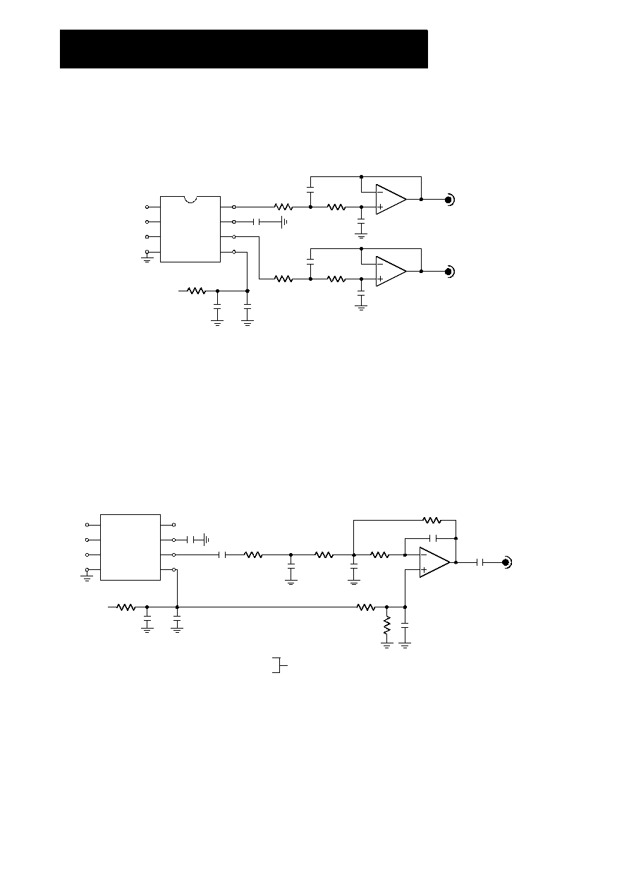
APPLICATION INFORMATION
Basic application example
A typical example of a CD-application with the MS6313 is shown in Fig.4. It features typical decoupling components
and a second-order analog post-filter (smoothing filter) stage providing a line output.
BCK
WS
DATA
GND
VoR
Cap
VoL
V
DD
MS6313
50k
MS6308
50k
420pF
10
V
DD
47uF
0.1uF
50k
MS6308
50k
420pF
100pF
100pF
1
2
3
4
5
6
7
8
Headphone
(32O)
Headphone
(32O)
10uF
Fig.4 Example of a 2nd order filter application.
Note :
No external capacitor loading is allowed at the output pins 6 and 8.
MP3 digital to analog converting solution. Fig.5 , 6
BCK
WS
DATA
GND
VoR
CAP
VoL
V
DD
MS6313
100uF
MS6308
68pF
56k
22k
22k
1nF
15k
1.2nF
1uF
100k
1uF
100k
10
V
DD
V
REF
47uF
0.1uF
10uF
f
-3dB
= 17.5kHz
DC
gain
= 1.5
V
DAC out p-p
= 1.32V
V
out p-p
= 1.98V
For V
DD
= 3.3V
Headphone
(32)
Fig.5 A third order lowpass filter ( Smoothing filter ) for DAC output.