 | –≠–ª–µ–∫—Ç—Ä–æ–Ω–Ω—ã–π –∫–æ–º–ø–æ–Ω–µ–Ω—Ç: MS6323TGU | –°–∫–∞—á–∞—Ç—å:  PDF PDF  ZIP ZIP |
Document Outline
- ˛ˇ
- ˛ˇ
- ˛ˇ
- ˛ˇ
- ˛ˇ
- ˛ˇ
- ˛ˇ
- ˛ˇ
- ˛ˇ
MO
SA
MS6323
16-Bits Stereo Audio DAC
REV1.1
1
www.mosanalog.com
16-Bits Stereo Audio DAC
Low Power Consumption
Low Voltage, Excellent PSRR
FEATURES
Operation range: 2.7V~5.5V
Excellent Power Supply Rejection Ratio(PSRR)
Low operating current
Low power consumption
8mW at V
DD
=3.3V (Full scale output )
Low distortion
No zero crossing distortion
Wide dynamic range(16-bit resolution)
Voltage Output
Fast setting time permits 2*, 4*, and 8* oversampling
(serial input) or double speed operation at 4*
oversampling
Compatible with most of the Japanese input formats;
time multiplexed, two's complement, CMOS and TTL
input level, MS6323AS for CMOS level, MS6323T for
TTL level
Output voltage swing is proportional to supply voltage
(V
OPP
=V
DD
/2)
Cost efficient
Space saving package SOP8, MSOP8
APPLICATIONS
Multimedia system
MP3, PDA, Portable Digital Audio.
DESCRIPTION
The MS6323 is a 16-bit voltage-output Digital-to-Analog Converter(DAC). It gives the excellent Power Supply
Rejection Ratio(PSRR). It features extremely low power dissipation, small package size and easy application. The
accuracy of the weight current sources, combined with the unique symmetrical decoding method, preclude zero-
crossing distortion and ensures high quality audio reproduction. These unique features, combined with its exceptional
performance, make the MS6323 ideally suited for use in portable audio equipment. MS6323 is pin and function
compatible with MS6313.
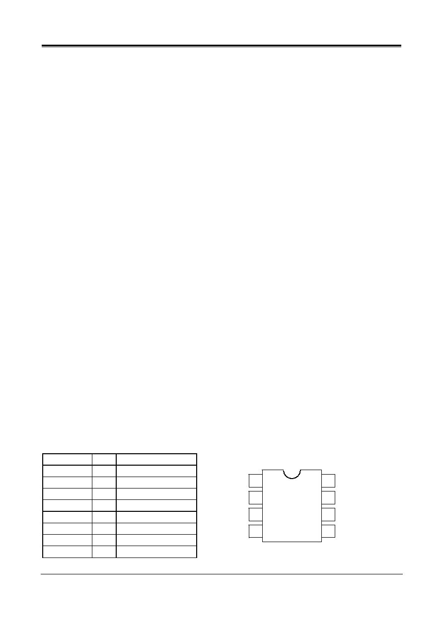
PIN CONFIGURATION
Symbol Pin
Description
BCK
1
Bit clock input
WS
2
Word select input
DATA 3 Data
input
GND 4
Ground
V
DD
5
Positive supply voltage
V
OL
6
Left channel output
Cap 7
Cap
V
OR
8 Right
channel
output
7
6
5
8
2
3
4
1
MS6323
V
OR
Cap
V
OL
V
DD
BCK
WS
DATA
GND
Pin 7 : Capacitor = 1
F (ripple rejection)
MO
SA
MS6323
16-Bits Stereo Audio DAC
REV1.1
2
www.mosanalog.com
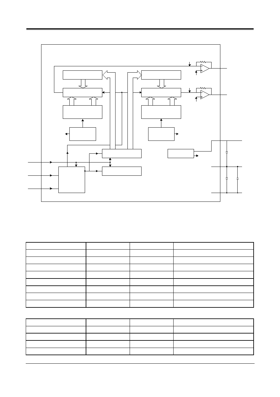
BLOCK DIAGRAM
LEFT OUTPUT LATCH
RIGHT OUTPUT LATCH
LEFT BIT SWITCHS
RIGHT BIT SWITCHS
16-BIT WEIGHT
CURRENT DIVIDER
16-BIT WEIGHT
CURRENT DIVIDER
LEFT INPUT LATCH
RIGHT INPUT LATCH
CONTROL
&
TIMING
BCK
WS
DATA
REFERENCE
SOURCE
1
2
3
4
5
V
DD
GND
10uF
R
F
I
BR
R
F
I
BL
V
REF
V
REF
V
OUT
LEFT
6
8
V
OUT
RIGHT
OP1
OP2
V
REF
0.1uF
7
1uF
CAP
REFERENCE
CURRENT
SOURCE
I
REF
I
BR
REFERENCE
CURRENT
SOURCE
I
REF
I
BL
Fig.1 Block diagram.
ORDERING INFORMATION
CMOS input level
Package Part
number
Packaging Marking
Transport Media
8-Pin SOP
MS6323ASTR
MS6323AS
2.5k Units Tape and Reel
8-Pin SOP
MS6323ASU
MS6323AS
100 Units Tube
8-Pin SOP (lead free)
MS6323ASGTR
MS6323ASG
2.5k Units Tape and Reel
8-Pin SOP (lead free)
MS6323ASGU
MS6323ASG
100 Units Tube
8-Pin MSOP
MS6323ASMTR
6323
3.5k Units Tape and Reel
8-Pin MSOP
MS6323ASMU
6323
80 Units Tube
8-Pin MSOP (lead free)
MS6323ASMGTR
6323G
3.5k Units Tape and Reel
8-Pin MSOP (lead free)
MS6323ASMGU
6323G
80 Units Tube
TTL input level
Package Part
number
Packaging Marking
Transport Media
8-Pin SOP (lead free)
MS6323TGTR
MS6323TG
2.5k Units Tape and Reel
8-Pin SOP (lead free)
MS6323TGU
MS6323TG
100 Units Tube
8-Pin MSOP (lead free)
MS6323TMGTR
6323TG
3.5k Units Tape and Reel
8-Pin MSOP (lead free)
MS6323TMGU
6323TG
80 Units Tube
MO
SA
MS6323
16-Bits Stereo Audio DAC
REV1.1
3
www.mosanalog.com
ABSOLUTE MAXIMUM RATINGS
Symbol
Parameter Rating
Unit
V
DD
Positive
Supply
Voltage
6
V
V
ESD
Electrostatic Handling
-2000 to 2000
V
T
STG
Storage Temperature Range
-65 to 150
T
A
Operating Ambient Temperature Range
-40 to 85
T
J
Maximum Junction Temperature
150
T
S
Soldering Temperature, 10 seconds
260
R
THJA
Thermal Resistance from Junction to Ambient in Free Air
SOP8
MSOP8
210
235
/W
OPERATING RATINGS
Symbol Parameter Min Typ Max Unit
V
DD
Supply
Voltage
2.7 - 5.5 V
3.3V ELECTRICAL CHARACTERISTICS
(Ta=25, V
DD
=3.3V, V
SS
=0V, f=1kHz, Cap=1uF; unless otherwise specified)
Symbol Parameter
Conditions Min
Typ
Max
Unit
DC Characteristics
V
CAP
Voltage at CAP
1.60
1.65
1.70
V
V
DC
Output DC level
1.60
1.65
1.70
V
V
FS
Full scale output voltage
V
FS
=0.5V
DD
1.5 1.65 1.8 Vpp
I
Q
Quiescent current
At code 0000H
-
2.0
2.3
mA
CAP=1uF, f=100Hz
45
50
-
dB
PSRR
Power supply rejection ratio
CAP=10uF, f=100Hz
63
68
-
dB
CS Channel
separation
78 84 - dB
AC Characteristics
Res Resolution
-
- 16 bits
- -66 -62 dB
THD+N
Total harmonic distortion plus
noise
- 0.05
0.08
%
S/N Signal-to-noise
ratio
86 92 - dB
MO
SA
MS6323
16-Bits Stereo Audio DAC
REV1.1
4
www.mosanalog.com
2.7V ELECTRICAL CHARACTERISTICS
(Ta=25, V
DD
=2.7V, V
SS
=0V, f=1kHz, Cap=1uF; unless otherwise specified)
Symbol Parameter
Conditions Min
Typ
Max
Unit
DC Characteristics
V
CAP
Voltage at CAP
1.30
1.35
1.40
V
V
DC
Output DC level
V
FS
=0.5V
DD
1.30 1.35 1.40 V
V
FS
Full scale output voltage
1.2
1.35
1.5
Vpp
I
Q
Quiescent current
At code 0000H
-
1.9
2.2
mA
CAP=1uF, f=100Hz
45
49
-
dB
PSRR
Power supply rejection ratio
CAP=10uF, f=100Hz
63
68
-
dB
CS Channel
separation
77 83 - dB
AC Characteristics
Res Resolution
-
- 16 bits
- -66 -62 dB
THD+N
Total harmonic distortion plus
noise
- 0.05
0.08
%
S/N Signal-to-noise
ratio
84 90 - dB
TYPICAL PERFORMANCE CHARACTERISTICS
(Ta=25, f=1kHz, Cap=1uF, sampling rate=4fs; unless otherwise specified, )
QUIE
S
C
E
N
T CURRE
NT (mA
)
SUPPLY VOLTAGE (V)
THD+N (%)
SUPPLY VOLTAGE (V)
C
H
AN
N
EL SEP
AR
ATI
O
N
(
d
B)
FREQUENCY (Hz)
Quiescent current vs. supply voltage e
THD+N vs. supply voltage
Channel separation vs. frequency
PSR
R
(
d
B)
FREQUENCY (Hz)
PSR
R
(
d
B)
FREQUENCY (Hz)
THD+N (%)
FREQUENCY (Hz)
PSRR vs. frequency
CAP=22uF
CAP=10uF
CAP=22uF
CAP=10uF
V
DD
=2.7V
CAP=1uF
CAP=1uF
V
DD
=3.3V
V
DD
=3.3V
V
RR
=-20dBV
V
DD
=2.7V
V
RR
=-20dBV
PSRR vs. frequency
THD+N vs. frequency
MO
SA
MS6323
16-Bits Stereo Audio DAC
REV1.1
5
www.mosanalog.com
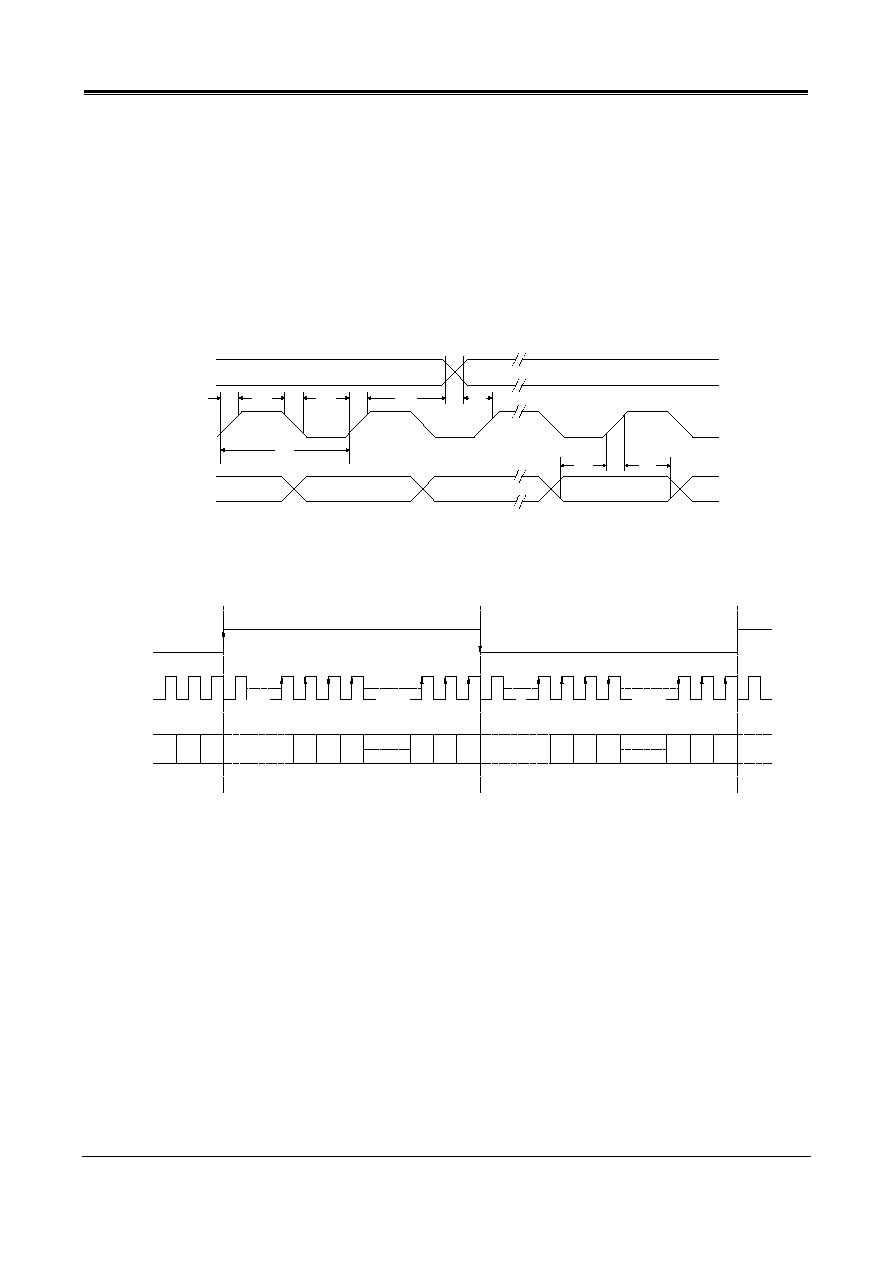
TIMING AND DATA FORMAT
The MS6323 accepts input serial data formats of 16-bit word length. Left and right data words are time
multiplexed. The MSB must always be first. The format of data input is shown in Figs. 2 and 3. With a HIGH level on
the word select input (WS), data is placed in the left input register and with LOW level on the WS input, data is placed
in the right register (Fig. 1). The data in the input registers are simultaneously latched in the output registers which
control the bit switches. Internal bias currents I
BL
and I
BR
are each added to the full scale output current I
FS
in order to
achieve the maximum dynamic range at the outputs of OP1 and OP2(Fig. 1). In this way the maximum dynamic range
is achieved over the entire power supply range.
RIGHT
WS
BCK
DATA
LSB
MSB
t
r
t
HB
t
f
t
cr
t
LB
t
HW
t
SW
LEFT
t
SD
t
HD
Fig.2 Timing and input signals.
0
1
2
15
14
13
2
1
0
MSB
LSB
15
14
13
2
1
0
MSB
LSB
RIGHT
LEFT
WS
BCK
DATA
Fig.3 Format of input signals.