MOSEL-VITELIC
MS62256H
MS62256H
32K x 8 HIGH SPEED
CMOS STATIC RAM
Features
s
High-speed ≠ 15/20/25/35 ns
s
Low Power dissipation:
MS62256HL
1.1W (Max.) Operating
1mW (Max.) Power down
s
Fully static operation
s
All inputs and outputs directly TTL compatible
s
Three state outputs
s
Ultra low data retention supply current at
V
CC
= 2V
Description
The MS62256H is a 262,144-bit static random
access memory organized as 32,768 words by 8
bits and operates from a single 5 volt supply. It is
built with MOSEL-VITELIC's high performance twin
tub CMOS process. Inputs and three-state outputs
are TTL compatible and allow for direct interfacing
with common system bus structures. The
MS62256H is available in the following standard
28-pin packages:
600 MIL Plastic DIP
300 MIL Plastic DIP
300 MIL Small Outline J-Bend (SOJ)
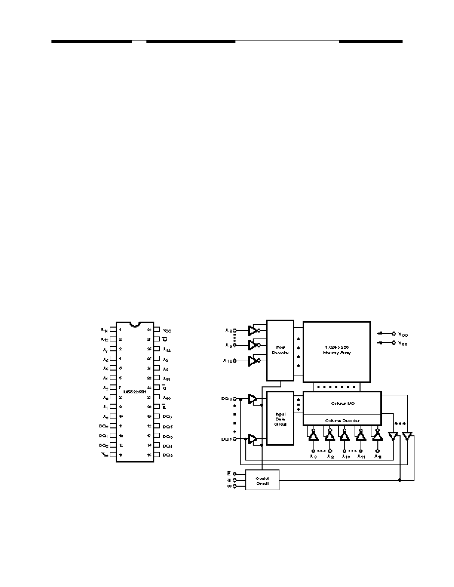
Pin Configurations
Functional Block Diagram
ADVANCED
INFORMATION
MOSEL-VITELIC
MS62256H
Pin Descriptions
A
0
- A
14
Address Inputs
These 15 address inputs select one of the 32768
8-bit words in the RAM.
E
Chip Enable Input
E is active LOW. The chip enable must be active
to read from or write to the device. If it is not active,
the device is deselected and is in a standby power
mode. The DQ pins will be in the high-impedance
state when deselected.
G
Output Enable Input
The output enable input is active LOW. If the
output enable is active while the chip is selected
and the write enable is inactive, data will be present
on the DQ pins and they will be enabled. The DQ
pins will be in the high impedance state when G is
inactive.
W
Write Enable Input
The write enable input is active LOW and controls
read and write operations. With the chip enabled,
when W is HIGH and G is LOW, output data will be
present at the DQ pins; when W is LOW, the data
present on the DQ pins will be written into the
selected memory location.
DQ
0
- DQ
7
Data Input/Output Ports
These 8 bidirectional ports are used to read data
from or write data into the RAM.
V
CC
Power Supply
V
SS
Ground
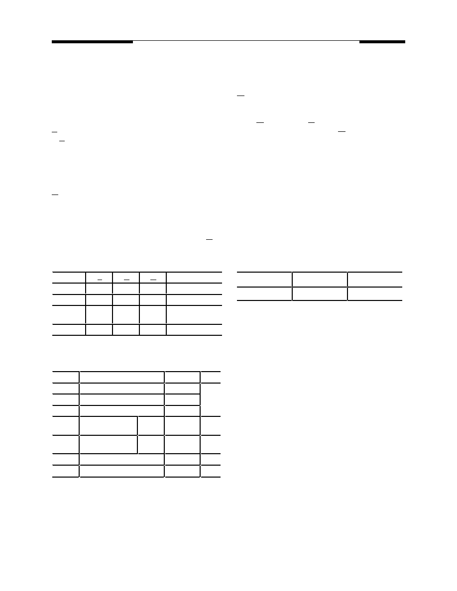
Truth Table
Operating Range
Range
Ambient
Temperature
V
cc
Commercial
0∞C to +70∞C
5V ± 10%
Mode
E
G
W
I/O Operation
Standby
H
X
X
High Z
Read
L
L
H
D
OUT
Output
Disabled
L
H
H
High Z
Write
L
X
L
D
IN
Absolute Maximum Ratings
(1)
Symbol
Parameter
Rating
Units
V
CC
Supply Voltage
-0.3 to 7
V
IN
Input Voltage
-0.3 to 7
V
V
DQ
Input/Output Voltage Applied
-0.3 to 6
T
BIAS
Temperature Under
Bias
Plastic
-10 to +125
∞C
T
STG
Storage
Temperature
Plastic
-40 to +150
∞C
P
D
Power Dissipation
1.2
W
I
OUT
DC Output Current
50
mA
1.
Stresses greater than those listed under ABSOLUTE
MAXIMUM RATINGS may cause permanent damage to
the device. This is a stress rating only and functional
operation of the device at these or any other conditions
above those indicated in the operational sections of this
specification is not implied. Exposure to absolute
maximum rating conditions for extended periods may
affect reliability and degrade performance characteristics.

MOSEL-VITELIC
MS62256H
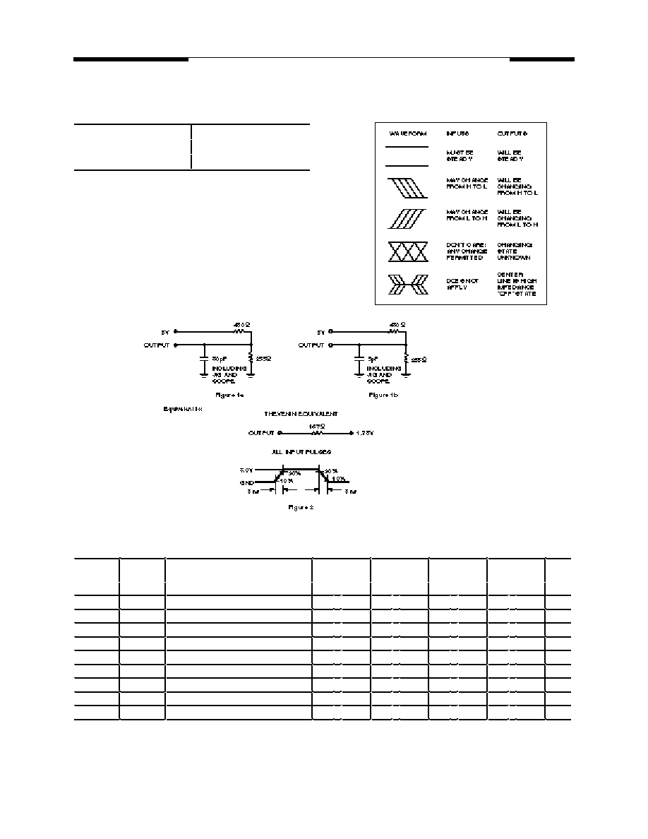
Capacitance
(1)
T
A
= 25∞C, f = 1.0MHz
1. This parameter is guaranteed and not tested.
Data Retention Characteristics (over the commercial operating range)
Timing Waveform Low V
CC
Data Retention Waveform
Symbol
Parameter
Conditions
Max.
Unit
C
IN
Input Capacitance
V
IN
= 0V
8
p F
C
I/O
Input/Output
Capacitance
V
I/O
= 0V
10
p F
DC Electrical Characteristics (over the commercial operating range)
1.
Typical characteristics are at V
CC
= 5V, T
A
= 25∞C.
2.
These are absolute values with respect to device ground and all overshoots due to system or tester noise are included.
3.
V
IL
(Min.) = ≠3.0V for pulse width
20ns
4.
F
MAX
= 1/t
RC.
5.
L version only.
Parameter
MS62256H
Name
Parameter
Test Conditions
Min.
Typ.
(1)
Max.
Units
V
IL
Guaranteed Input Low Voltage
(2,3)
≠0.3
-
0.8
V
V
IH
Guaranteed Input High Voltage
(2)
2.2
-
6.0
V
I
IL
Input Leakage Current
V
CC
= Max, V
IN
= 0V to V
CC
≠2
-
2
µ
A
I
OL
Output Leakage Current
V
CC
= Max, E = V
IH
or G = V
IH
, V
IN
= 0V t o V
CC
≠2
-
2
µ
A
V
OL
Output Low Voltage
V
CC
= Min, I
OL
= 8mA
-
-
0.4
V
V
OH
Output High Voltage
V
CC
= Min, I
OH
= -4.0mA
2.4
-
-
V
I
CC
Operating Power Supply Current V
CC
= Max, E
= V
IL
, I
DQ
= 0mA, F = F
m ax
(4)
-
-
200
mA
I
CCSB
Standby Power Supply Current
V
CC
= Max, E = V
IH
, I
DQ
= 0mA
-
-
40
mA
I
CCSB1
Power Down Power Supply
V
CC
= Max, E
V
CC
≠ 0.2V
-
-
2
mA
Current
V
IN
V
CC
≠ 0.2V or V
IN
0.2V
-
-
130
(5)
µA
Symbol
Parameter
Test Conditions
Min.
Typ.
(1)
Max
(2)
Units
V
DR
V
CC
for Data Retention
E
V
CC
≠ 0.2V, V
IN
V
CC
≠ 0.2V or V
IN
0.2V
2.0
(
-
-
V
I
CCDR
Data Retention Current
E
V
CC
≠ 0.2V, V
IN
V
CC
-≠ 0.2V or V
IN
0.2V
-
2
50
4)
µA
t
CDR
Chip Deselect to Data Retention
Time
See Retention Waveform
0
-
-
ns
t
R
Operation Recovery Time
t
RC
(3)
-
-
ns
1.
V
CC
= 2V, T
A
= +25∞C
2.
V
CC
= 3V
3.
t
RC
= Read Cycle Time
MOSEL-VITELIC
MS62256H
AC Electrical Characteristics (over the commercial operating range)
Read Cycle
AC Test Conditions
Input Pulse Levels
0V to 3.0V
Input Rise and Fall Times
3ns
Timing Reference Level
1.5V
Key to Switching Waveforms
AC Test Loads and Waveforms
Jedec
Parameter Parameter
MS62256H-15 MS62256H-20 MS62256H-25 MS62256H-35
Name
Name
Parameter
Min.
Max. Min.
Max. Min.
Max. Min.
Max. Unit
t
AVAX
t
RC
Read Cycle Time
15
-
20
-
25
-
35
-
ns
t
AVQV
t
AA
Address Access Time
-
15
-
20
-
25
-
35
ns
t
ELQV
t
ACS
Chip Enable Access Time
-
15
-
20
-
25
-
35
ns
t
GLQX
t
OE
Output Enable to Output Valid
-
8
-
10
-
12
-
15
ns
t
EHQZ
t
CLZ
Chip Enable to Output Low Z
5
-
5
-
5
-
5
-
ns
t
GLQX
t
OLZ
Output Enable to Output in Low Z
0
-
0
-
0
-
0
-
ns
t
EHQZ
t
CHZ
Chip Disable to Output in High Z
-
8
-
8
-
10
-
15
ns
t
GHQZ
t
OHZ
Output Disable to Output in High Z
-
8
-
8
-
10
-
15
ns
t
AXQX
t
OH
Output Hold from Address Change
3
-
5
-
5
-
5
-
ns

MOSEL-VITELIC
MS62256H
READ CYCLE 2
(1, 2, 4)
READ CYCLE 3
(1, 3, 4)
NOTES:
1.
W is High for READ Cycle.
2.
Device is continuously selected E = V
IL
.
3.
Address valid prior to or coincident with E transition low.
4.
G = V
IL
.
5.
Transition is measured ± 500mV from steady state with C
L
= 5pF as shown in Figure 1b. This parameter is guaranteed and not
100% tested.
Switching Waveforms (Read Cycle)
READ CYCLE 1
(1)