 | –≠–ª–µ–∫—Ç—Ä–æ–Ω–Ω—ã–π –∫–æ–º–ø–æ–Ω–µ–Ω—Ç: MSS0605 | –°–∫–∞—á–∞—Ç—å:  PDF PDF  ZIP ZIP |

MOSEL VITELIC
1
PID225B 04/94
MSS0605
MOSEL
APRIL
VOICE ROM
Block Diagram
Features
Single power supply can operate at 2.4V
through 6V.
Current output can drive 8 ohm speaker with
a transistor, Vout can drive buzzer directly.
The voice content is stored up to 6 seconds
and can be separated to 9 sections.
Nine trigger input pins are provided. Each
trigger pin can access a phrase instead of
simple section. A phrase is composed of one
or more than one section(s) and called a
section - combination of sections.
Total section number of all phrases is up to 64.
Total duration of all sections with mute is up
to 24 seconds.
Interrupt function (INTP) stops the audio output
at once.
Playall function (OKY) plays all 9 phrases one
by one by single trigger.
Sequential function (OKY): one trigger plays
next phrase of 9 phrases circularly.
2 LED function with 6 or 3 Hz flash is provided
to tell the audio status in alternate flash.
A STOP pulse comes out when audio signal is
finished.
CDS input interface with debounce is provided for
9 trigger pins, OKY pin and INTP pin.
Extra pad for REPeat playing.
Mask option for either real Busy or Ground
Busy on BUSY signal.
Mask option for 10ms, 0.4ms, 10us on debounce
time.
Mask option for either PLAYALL or SEQUENTIAL
for one-key function.
Separate option setting on 9 individual trigger
pins and OKY pin for below four masks:
a. Mask option for either Level or Edge trigger
type.
b. Mask option for either Holdable or Unholdable
output type.
c. Mask option for either BUSY output or STOP
pulse on STBZ output.
d. Mask option for either Retrigger or Irretrigger .
Description
The MSS0605 is a monolithic CMOS VLSI ASIC that can memorize voice up to 6 seconds using
MOSEL qualified coding method (MPCM). It can play 9 phrases instead of 9 simple sections. Most
of the necessary circuit are built in like oscillator, ROM, DAC and interface logic. 2 LEDs and
separate option setting is provided . Customer voice data will be edited and built in by mask
programming during the device fabrication.
CLOCK
GENERATOR
CONTROL
LOGIC
TG0
TG1
TG2
TG3
OKY
INTP
REP
LED 1
OSC
TIMING
GENERATOR
ADDRESS
GENERATOR
VOICE
ROM
TRIGGER
TABLE
MPCM
DECODER
CURRENT
BUFFER
BUZZER
BUFFER
C
OUT
V
OUT1
V
OUT2
V
DD
V
SS
TG4
TG5
TG6
TG7
TG8
LED 2
STBZ
Contact your sales representative for the most recent information
∑\ÿ
∞
G
ß@ßuþ@
qø£®
2.4
∑“ÿS
∞
,,6.0∑“ÿS
∞
C
∑i∑H
±
ø
°™‘Ê
©OE¨´•
»
±
ø
8
,∑z
∞
C
ßE®q°n
µ
ß
∆e,ÆC®qTMØ¥
∑iߣ∂P,ßE®qß
∆e°`TMØ¥
®
6®Ã
∞
ÆC®q™y
µ±
aøR
µ
∆...
∞
TMØ¥
∑i
F24®Ã
∞
C
∂
ß@
"™y
µ
ß”¥H
™P∂£
L¥H
∂@∑OE¯
∑i
z
L∑
±
"
qTM
£∑’
µ
o¥H
∂b
}®O∂£
L¥H
∆...∑i
z
L∑
n¯‘Ê<∑¯∂V∂£
L¥H
∂œ¯»∑X
∞
C
∂
Æ,
"
µ
o∑ßG
∑
»¯»∑X
}
∞
A∑i
z
L∑
n¯‘Ê<©T©wøW
v(ÆC
®Ã6∂
©OE3∂
©
ø)TM
ßÀ∂
∞∞
C
∑i
z
L∑
n¯‘Ê<
10ms,0.4ms,10us
ßT
ˇ
µ
o
T™{∆...
∞
ÆC
"
µ
o°∑i∂U∂§¯W∑fl
z
L∑
n¯‘Ê<
∞
]∑"
∞
^
q∑
µ
o©OE®O
t
µ
o
∞
]ßA
∞
^þQ∑OE
µ
o¥H
ßþTMØ
µ
u•x
±±
™y
µ
¯»∑Xßþ
±
™Pþ_©OE®Oß
(Unholdable)
∞
]ß
∞
^™y
µ
ß”¯»∑XÿflÆR©OE®Oߣ
n
∞
]ßB
∞
^∑i∑H
Q¥∑®q™\
±
∫©OE®Oߣ
n
∂
ßE
"¥^°∑i∑H©“∑XßE∑y
<
∞
AÆC∑y
<∑i∑H∑--ßW
±
ßE
∑Ÿ
N
'∂Æ
∞
C
∑i
z
L∑
n¯‘Ê<
°∑
∞
©“
µ
(Playall)
°
vß@©“
µ
(Playnext)
∞
C
Æ∑L∑\ÿ
≠
`∑™∑€∑L
B™
∞
©
MOSEL VITELIC
Pad Description
2
PID225B 04/94
MSS0605
MOSEL
DC Characteristics
Symbol
Parameter
Min.
Max.
Typ.
Unit
Condition
I
I
I
I
F/F
Supply
Current
Stand by
Operating
O/P Current
V
,V
Output Current (C )
Frequency Stability
Drive
Sink
µ
A
V = 4.5V, I/O Open
DD
SB
OP
OH
OL
OUT1
OUT2
-13
13
5
1
200
mA
%
I
CO
DD
V = 0V
O/P
V = 4.5V,
V = 4.5V
O/P
V = 4.5V,
DD
F
OSC
(4.5V) - F
OSC
(4V)
F
OSC
(4.5V)
DD
V = 4.5V, R
OSC
= 1.2M
I
I
Input Current
IH
IL
10
µ
A
DD
V = 4.5V
TG0~TG8, OKY,
INTP, REP
OUT
2.5
F/F
Fosc Variation
10
%
Pad No.
Signal Name
Function
1
2
3
4
5
6
7
8
I/O
9
10
11
12
13
14
15
16
17
18
19
I
Output Current
STOP / BUSY
OH
-8
8
mA
I
OL
V = 0V
O/P
V = 4.5V,
DD
V = 4.5V
O/P
V = 4.5V,
DD
V = 0V
O/P
V = 3V,
DD
20
INTP
I
Interrupt input, internal pull low, high active
OKY
One key function input, internal pull low, hgih active
I
TG5
I
I
TG8
TG6
TG7
Trigger 8 input, internal pull low, high active
Trigger 7 input, internal pull low, high active
Trigger 6 input, internal pull low, high active
Trigger 5 input, internal pull low, high active
I
I
TG1
I
I
I
TG4
TG2
TG3
Trigger 4 input, internal pull low, high active
TG0
Trigger 3 input, internal pull low, high active
Trigger 2 input, internal pull low, high active
Trigger 1 input, internal pull low, high active
Trigger 0 input, internal pull low, high active
I
I
V
DD
OSC
Positive power supply
Oscillator Resistor input
I
Power
C
OUT
O
Audio signal current output (for speaker)
V
OUT1
O
V
OUT2
Audio signal voltage output (for buzzer)
Audio signal voltage output (for buzzer)
O
21
22
V
SS
Negative power supply
Power
REP
I
High use as repeat
NC
NC
No connection
STBZ
O
One shot stop signal output / BUSY signal output
LED 1
LED 2
O
O
LED signal output , sink current output.
5.0
0
V = 0V
O/P
V = 6.0V,
DD
V = 4.5V
O/P
V = 4.5V,
DD
I
OL
Output Current
LED1 ,LED2
13
mA
0.1
3.8
V = 0V
O/P
V = 4.5V,
DD
mA

MOSEL VITELIC
MSS0605
I. Edge/Unholdable/Retrigger Trigger Mask
a. When trigger is shorter than a whole section output
b. When trigger is longer than a whole section output
TG2
AUDIO
LED's
II. Level/Unholdable/Retrigger Trigger Mask
a. When trigger is shorter than a whole section output
b. When trigger is longer than a whole section output
Timing Diagram
3
PID225B 04/94
TG2
AUDIO
LED's
Phrase2
TG1
STOP
STOP
a. When trigger is shorter than a whole section output
b. When trigger is longer than a whole section output
III. Edge/Holdable/Retrigger Trigger Mask
TG2
AUDIO
LED's
TG1
STOP
Absolute Maximum Rating
C
Symbol
T (Operating)
T (Storage)
V ~ V
DD
SS
V
IN
V
OUT
Rating
-0.5 ~ +7.0
-10 ~ +60
-55 ~ +125
V -0.3 < V < V +0.3
SS
IN
DD
V <V < V
OUT
SS
DD
Unit
V
V
V
C
AC Characteristics
Timing
Unit
T
STOP
Stop pulse
Phrase2
Phrase2
Phrase2
Phrase2
Phrase1
Phrase2
Phrase2
Phrase2
Phrase2
Phrase1
Min.
Max.
20
ms
Typ.
BUSY
BUSY
BUSY
T
P
T R
Power rise up time
Power Ripple width
1
1
ms
ms

MOSEL VITELIC
MSS0605
4
PID225B 04/94
IV. Level/Holdable/Retrigger Trigger Mask
a. When trigger is shorter than a whole section output
b. When trigger is longer than a whole section output
TG2
AUDIO
TG1
V. One Key Pin Play All Function
One Key
AUDIO
VI. One Key Pin Sequential Play Function
One Key
AUDIO
Phrase2
Phrase2
Phrase1
Phrase2
Phrase0
Phrase1
PhraseN
Phrase0
Phrase1
Phrase2
LNEP
Phrase0
a.EDGE / UNHOLD
Phrase0
One Key
AUDIO
Phrase0
Phrase1
PhraseN
PhraseN
b.LEVEL / UNHOLD
Phrase0
Phrase0
One Key
AUDIO
Phrase0
Phrase1
c.EDGE / HOLD
Phrase0
One Key
AUDIO
Phrase0
Phrase1
d.LEVEL / HOLD
Phrase0
Phrase0
One Key
AUDIO
Phrase0
Phrase1
e.RETRIGGER
Phrase2
One Key
AUDIO
Phrase0
Phrase1
Phrase2
Phrase1
e.RETRIGGER
Phrase0
Phrase2
a.EDGE / UNHOLD
b.LEVEL / UNHOLD
One Key
AUDIO
Phrase0
Phrase1
Phrase1
Phrase0
Phrase1
One Key
AUDIO
Phrase0
Phrase1
Phrase0
c.EDGE / HOLD
d.LEVEL / HOLD
One Key
AUDIO
Phrase0
Phrase1
Phrase1
Phrase0
Phrase1
LNEP = The last Non-Empty Phrase
LNEP
LNEP
LNEP
LNEP
LNEP
LNEP
LNEP
LNEP

MOSEL VITELIC
MSS0605
5
PID225B 04/94
VII. Interrupt Pin Function
TG1
AUDIO
Interrupt
Phrase
Phrase
Phrase
1. Typical Application
Application Circuit
AUDIO
Phrase0
TG0
REP
VIII. Repeat funtion
Phrase0
Phrase0
Phrase0
PID SIZE = 90 X 90 um
NOTE : * SUBTRATE is V
DD
TG
AUDIO
T
T
IX. DEBOUNCE TIME
( 3 optional intervals )
X. Acceptable Power On Signal & Ripple
T
P
90% V
DD
10% V
DD
90% V
DD
T
R
V
SS = 0.0 V
V
DD
TG0
TG1
TG2
TG3
TG4
TG5
TG6
TG7
TG8
OKY
INTP
REP
Vss
STBZ
V1
V2
Cout
V
DD
R1
LED2 LED1
R2
MOSEL VITELIC
MSS0605
6
PID225B 04/94
T
S
VDD
VSS
COUT
VDD
VSS
COUT
TG0
TG1
TG2
TG3
TG4
TG5
TG6
TG7
TG8
INTP
OKY
REP
OSC
R1
TG0
TG1
TG2
TG3
TG4
TG5
TG6
TG7
TG8
INTP
OKY
REP
OSC
R1'
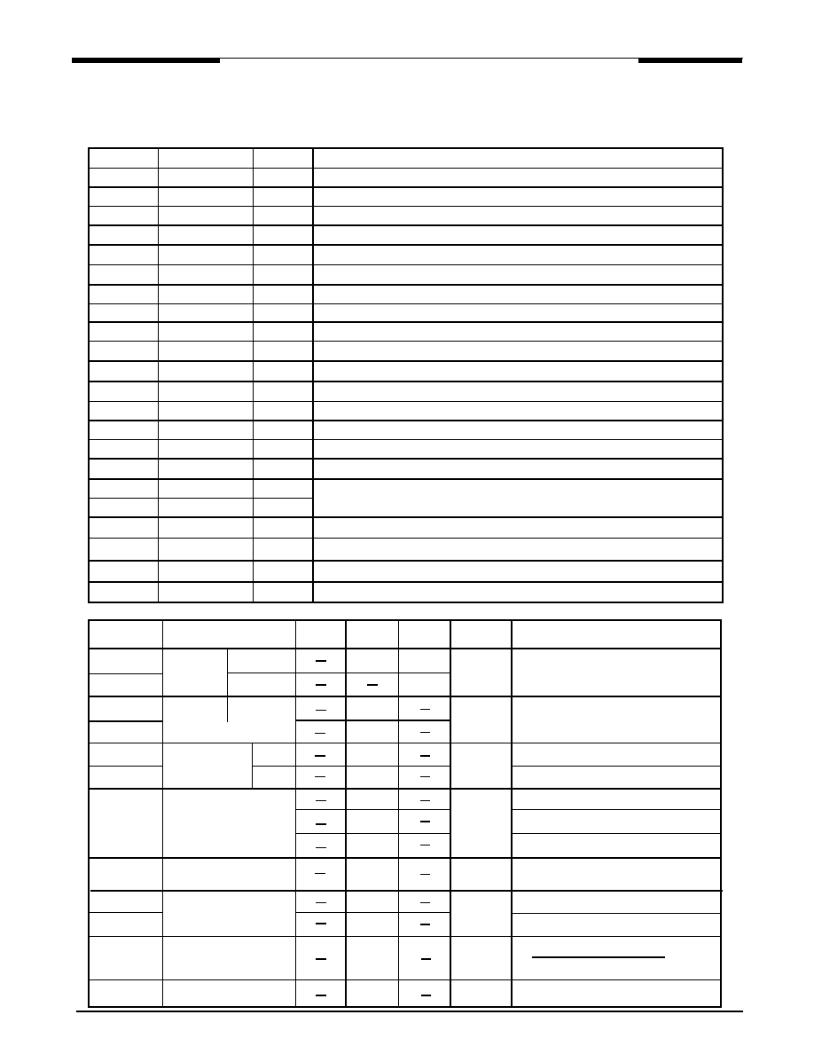
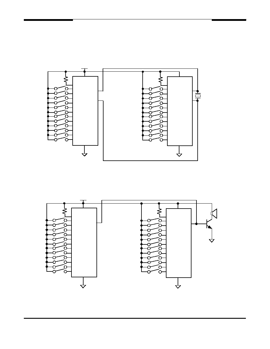
2. Parallel Application
VDD
VSS
VOUT1
VOUT2
VDD
VSS
PIEZO
BUZZER
VOUT1
VOUT2
TG0
TG1
TG2
TG3
TG4
TG5
TG6
TG7
TG8
INTP
OKY
REP
OSC
R1
TG0
TG1
TG2
TG3
TG4
TG5
TG6
TG7
TG8
INTP
OKY
REP
OSC
R1'

MOSEL VITELIC
MSS0605
7
PID225B 04/94
VDD
VSS
OSC
R1'
T
S
COUT
VDD
VSS
OSC
R1
COUT
STP
TG
Interrupt
TG
Interrupt
4. CDS Application
VDD
VSS
TG
OSC
R1
T
S
COUT
Reserves the right to make changes to above content and product without notice .
Note: 1. R1 = 1.2 M
, T(transistor) = þ > 130, R2 = 470
, S(speaker) = 1/4 w, 8
; all typical.
2. R2=470
( typical ) to bypass extra current into base to get rid of waveform saturation
on collector .
3. Piezo buzzer resonant frequency being around 1K Hz is recommended.
4. Input switch could be replaced by CDS.
5.COUT,VOUT1,VOUT2 are tristate during stand by state.
5. Edge Mode Change To Level Mode for TG0
VDD
VSS
COUT
TG0
OSC
R1
T
S
( The pin " REP " connects to VDD )
REP
3. Cascade Application
MOSEL
No. 1, R&D I Rd., Hsinchu Science-Based Industrial Park, Hsinchu,
Taiwan, R.O.C.
TEL:886-3-577-0055 FAX:886-3-577-2788
3910 North First street, San Jose, CA 95134-1501 U.S.A.
TEL:1-408-433-6000 FAX:1-408-433-0952
Service phone :
886-3-5784732