
MOSEL VITELIC
1
V29C51000T/V29C51000B
512K BIT (65,536 x 8 BIT)
5 VOLT CMOS FLASH MEMORY
PRELIMINARY
V29C51000T/V29C51000B Rev. 0.5 October 2000
Features
s
64Kx8-bit Organization
s
Address Access Time: 45, 70, 90 ns
s
Single 5V
±
10% Power Supply
s
Sector Erase Mode Operation
s
8KB Boot Block (lockable)
s
512 bytes per Sector, 128 Sectors
≠ Sector-Erase Cycle Time: 10ms (Max)
≠ Byte-Program Cycle Time: 20
µ
s (Max)
s
Minimum 10,000 Erase-Program Cycles
s
Low power dissipation
≠ Active Read Current: 20mA (Typ)
≠ Active Program Current: 30mA (Typ)
≠ Standby Current: 100
µ
A (Max)
s
Hardware Data Protection
s
Low V
CC
Program Inhibit Below 3.2V
s
Self-timed program/erase operations with end-
of-cycle detection
≠ DATA Polling
≠ Toggle Bit
s
CMOS and TTL Interface
s
Available in two versions
≠ V29C51000T (Top Boot Block)
≠ V29C51000B (Bottom Boot Block)
s
Packages:
≠ 32-pin Plastic DIP
≠ 32-pin TSOP-I
≠ 32-pin PLCC
Description
The V29C51000T/V29C51000B is a high speed
65,536 x 8 bit CMOS flash memory. Programming
or erasing the device is done with a single 5 Volt
power supply. The device has separate chip enable
CE, program enable WE, and output enable OE
controls to eliminate bus contention.
The V29C51000T/V29C51000B offers a combi-
nation of features: Boot Block with Sector Erase
Mode. The end of program/erase cycle is detected
by DATA Polling of I/O
7
or by the Toggle Bit I/O
6
.
The V29C51000T/V29C51000B features a
sector erase operation which allows each sector to
be erased and reprogrammed without affecting
data stored in other sectors. The device also
supports full chip erase.
Boot block architecture enables the device to
boot from either the top (V29C51000T) or bottom
(V29C51000B) sector. All inputs and outputs are
CMOS and TTL compatible.
The V29C51000T/V29C51000B is ideal for
applications that require updatable code and data
storage.
Device Usage Chart
Operating
Temperature
Range
Package Outline
Access Time (ns)
Temperature
Mark
P
T
J
45
70
90
0
∞
C to 70
∞
C
∑
∑
∑
∑
∑
∑
Blank

2
MOSEL VITELIC
V29C51000T/V29C51000B
V29C51000T/V29C51000B Rev. 0.5 October 2000
OPERATING VOLTAGE
51: 5V
DEVICE
SPEED
51000-01
V
29
C
000
51
BOOT BLOCK LOCATION
T: TOP
B: BOTTOM
T
≠
45: 45ns
70: 70ns
90: 90ns
BLANK (0
∞
C TO 70
∞
C)
P = PDIP
T = TSOP-I
J = PLCC
TEMP.
PKG.
Pin Configurations
N/C
N/C
A15
A12
A7
A6
A5
A4
A3
A2
A1
A0
I/O0
I/O1
I/O2
GND
1
2
3
4
5
6
8
9
10
11
12
13
14
15
16
30
31
32
29
28
27
26
25
7
24
23
22
21
20
32-Pin PDIP
Top View
V
CC
WE
NC
A14
A13
A8
A9
A11
OE
A10
CE
I/O3
I/O4
I/O5
I/O6
I/O7
19
18
17
51001-02
Pin Names
A
0
≠A
15
Address Inputs
I/O
0
≠I/O
7
Data Input/Output
CE
Chip Enable
OE
Output Enable
WE
Program Enable
V
CC
5V
±
10% Power Supply
GND
Ground
NC No
Connect
A
6
A
5
A
4
A
3
A
2
A
1
I/O
0
5
6
7
8
9
10
11
12
13
29
51001-03
28
27
26
25
24
23
22
21
A
12
A
15
NC
NC
V
CC
WE
NC
A
0
14
I/O
2
GND
I/O
3
I/O
4
I/O
5
I/O
6
A
7
A
13
A
8
A
9
A
11
OE
A
10
I/O
7
CE
A
14
I/O
1
32 Pin PLCC
Top View
15 16 17 18 19 20
4
3
2
1
32 31 30
A11
A9
A8
A13
A14
NC
WE
VCC
N/C
N/C
A15
A12
A7
A6
A5
A4
1
2
3
4
5
6
8
9
10
11
12
13
14
15
16
30
31
32
29
28
27
26
25
7
24
23
22
21
20
32-Pin TSOP I
Standard Pinout
Top View
OE
A10
CE
I/O7
I/O6
I/O5
I/O4
I/O3
GND
I/O2
I/O1
A3
A2
A1
A0
I/O0
19
18
17
51001-04
MOSEL VITELIC
V29C51000T/V29C51000B
3
V29C51000T/V29C51000B Rev. 0.5 October 2000
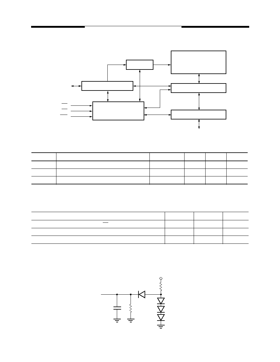
Functional Block Diagram
Capacitance
(1,2)
NOTE:
1.
Capacitance is sampled and not 100% tested.
2.
T
A
= 25
∞
C, V
CC
= 5V
±
10%, f = 1 MHz.
Latch Up Characteristics
(1)
NOTE:
1.
Includes all pins except V
CC
. Test conditions: V
CC
= 5V, one pin at a time.
AC Test Load
Symbol
Parameter
Test mSetup
Typ.
Max.
Units
C
IN
Input Capacitance
V
IN
= 0
6
8
pF
C
OUT
Output Capacitance
V
OUT
= 0
8
12
pF
C
IN2
Control Pin Capacitance
V
IN
= 0
8
10
pF
Parameter Min.
Max.
Unit
Input Voltage with Respect to GND on A
9
, OE
-1
+13
V
Input Voltage with Respect to GND on I/O, address or control pins
-1
V
CC
+ 1
V
V
CC
Current
-100
+100
mA
Address buffer & latches
A
0
≠A
15
51001-05
I/O Buffer & Data Latches
I/O
0
≠I/O
7
Y-Decoder
65,536 Bit
Memory Cell Array
X-Decoder
Control Logic
CE
OE
WE
51001-06
IN3064 or Equivalent
IN3064
or Equivalent
2.7 k
6.2 k
+5.0 V
IN3064 or Equivalent
IN3064 or Equivalent
C
L
= 100 pF
Device Under
Test
4
MOSEL VITELIC
V29C51000T/V29C51000B
V29C51000T/V29C51000B Rev. 0.5 October 2000
Absolute Maximum Ratings
(1)
NOTE:
1.
Stress greater than those listed unders "Absolute Maximum Ratings" may cause permanent damage to the device. This is a stress
rating only and functional operation of the device at these or any other conditions above those indicated in the operational sections
of this specification is not implied. Exposure to absolute maximum rating conditions for extended periods may affect reliability.
2.
No more than one output maybe shorted at a time and not exceeding one second long.
DC Electrical Characteristics
(over the commercial operating range)
Symbol
Parameter
Commercial
Unit
V
IN
Input Voltage (input or I/O pins)
-2 to +7
V
V
IN
Input Voltage (A
9
pin, OE)
-2 to +13
V
V
CC
Power Supply Voltage
-0.5 to +5.5
V
T
STG
Storage Temerpature (Plastic)
-65 to +125
∞
C
T
OPR
Operating Temperature
0 to +70
∞
C
I
OUT
Short Circuit Current
(2)
200 (Max.)
mA
Parameter
Name
Parameter
Test Conditions
Min.
Max.
Unit
V
IL
Input LOW Voltage
V
CC
= V
CC
Min.
--
0.8
V
V
IH
Input HIGH Voltage
V
CC
= V
CC
Max.
2
--
V
I
IL
Input Leakage Current
V
IN
= GND to V
CC
, V
CC
= V
CC
Max.
--
±
1
µ
A
I
OL
Output Leakage Current
V
OUT
= GND to V
CC
, V
CC
= V
CC
Max.
--
±
1
µ
A
V
OL
Output LOW Voltage
V
CC
= V
CC
Min., I
OL
= 2.1mA
--
0.4
V
V
OH
Output HIGH Voltage
V
CC
= V
CC
Min, I
OH
= -400
µ
A
2.4
--
V
I
CC1
Read Current
CE = OE = V
IL
, WE = V
IH
, all I/Os open,
Address input = V
IL
/V
IH
, at f = 1/t
RC
Min.,
V
CC
= V
CC
Max.
--
40
mA
I
CC2
Program Current
CE = WE = VIL, OE = V
IH
, V
CC
= V
CC
Max.
--
50
mA
I
SB
TTL Standby Current
CE = OE = WE = V
IH
, V
CC
= V
CC
Max.
--
2
mA
I
SB1
CMOS Standby Current
CE = OE = WE = V
CC
≠ 0.3V, V
CC
= V
CC
Max.
--
100
µ
A
V
H
Device ID Voltage for A
9
CE = OE = V
IL
, WE = V
IH
11.5
12.5
V
I
H
Device ID Current for A
9
CE = OE = V
IL
, WE = V
IH
, A9 = V
H
Max.
--
50
µ
A
MOSEL VITELIC
V29C51000T/V29C51000B
5
V29C51000T/V29C51000B Rev. 0.5 October 2000
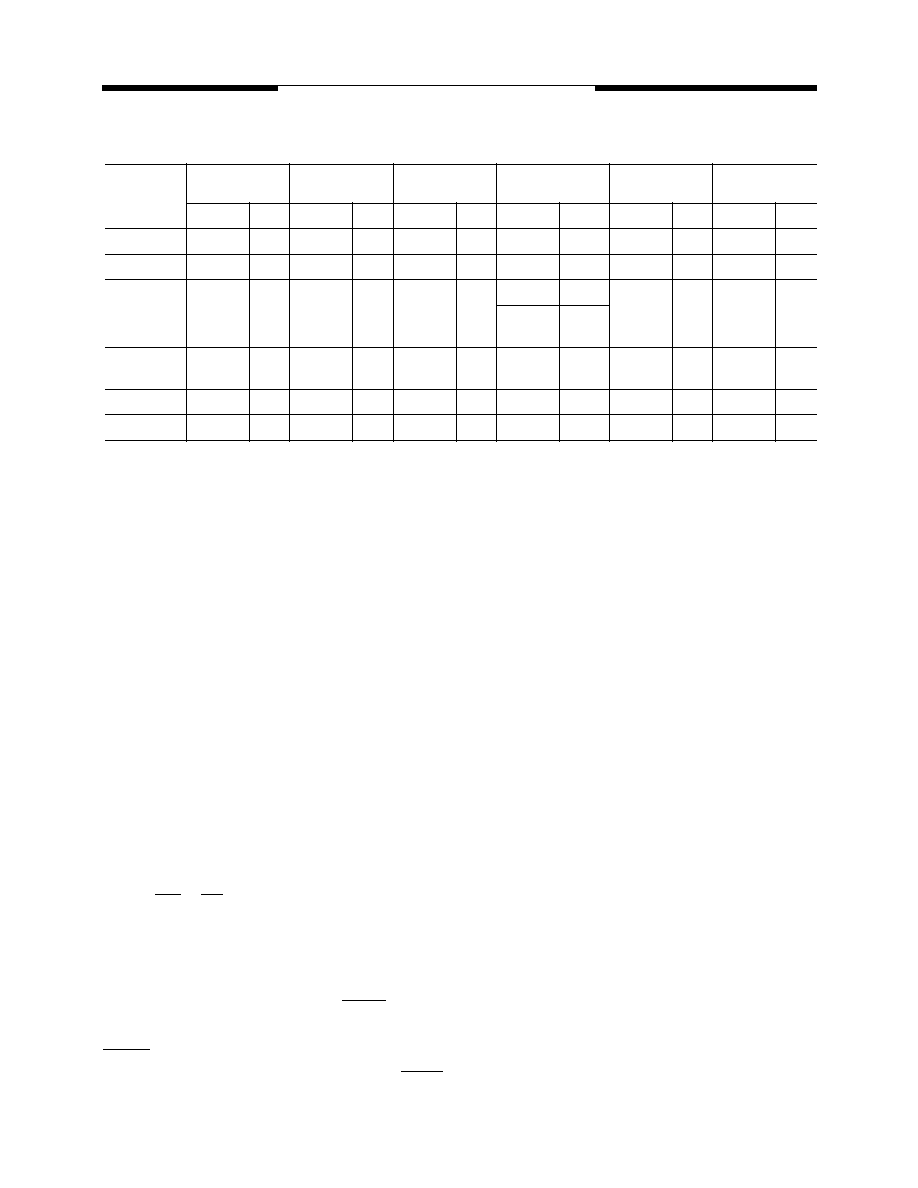
AC Electrical Characteristics
(over all temperature ranges)
Read Cycle
Program (Erase/Program) Cycle
Parameter
Name
Parameter
-45
-70
-90
Unit
Min.
Max.
Min.
Max.
Min.
Max.
t
RC
Read Cycle Time
45
--
70
--
90
--
ns
t
AA
Address Access Time
--
45
--
70
--
90
ns
t
ACS
Chip Enable Access Time
--
45
--
70
--
90
ns
t
OE
Output Enable Access Time
--
25
--
35
--
45
ns
t
CLZ
CE Low to Output Active
0
--
0
--
0
--
ns
t
OLZ
OE Low to Output Active
0
--
0
--
0
--
ns
t
DF
Output Enable or Chip Disable to Output in
High Z
0
20
0
20
0
30
ns
t
OH
Output Hold from Address Change
0
--
0
--
0
--
ns
Parameter
Name
Parameter
-45
-70
-90
Unit
Min. Typ. Max. Min. Typ. Max. Min. Typ. Max.
t
WC
Program Cycle Time
45
--
--
70
--
--
90
--
--
ns
t
AS
Address Setup Time
0
--
--
0
--
--
0
--
--
ns
t
AH
Address Hold Time
35
--
--
45
--
--
45
--
--
ns
t
CS
CE Setup Time
0
--
--
0
--
--
0
--
--
ns
t
CH
CE Hold Time
0
--
--
0
--
--
0
--
--
ns
t
OES
OE Setup Time
0
--
--
0
--
--
0
--
--
ns
t
OEH
OE High Hold Time
0
--
--
0
--
--
0
--
--
ns
t
WP
WE Pulse Width
25
--
--
35
--
--
45
--
--
ns
t
WPH
WE Pulse Width High
20
--
--
35
--
--
38
--
--
ns
t
DS
Data Setup Time
20
--
--
25
--
--
30
--
--
ns
t
DH
Data Hold Time
0
--
--
0
--
--
0
--
--
ns
t
WHWH1
Programming Cycle
--
--
20
--
--
20
--
--
20
µ
s
t
WHWH2
Sector Erase Cycle
--
--
10
--
--
10
--
--
10
ms
t
WHWH3
Chip Erase Cycle
--
500
--
--
500
--
--
500
--
ms
6
MOSEL VITELIC
V29C51000T/V29C51000B
V29C51000T/V29C51000B Rev. 0.5 October 2000
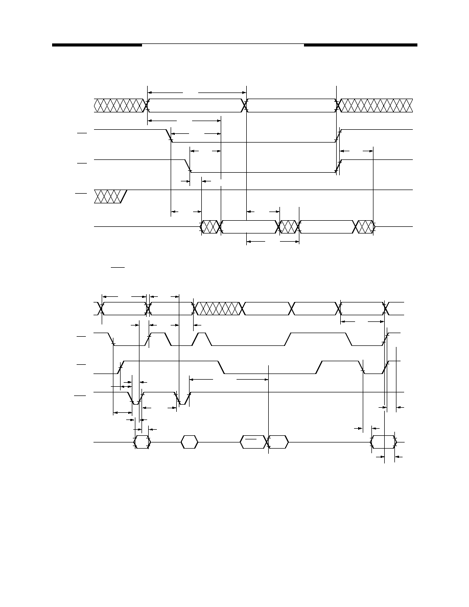
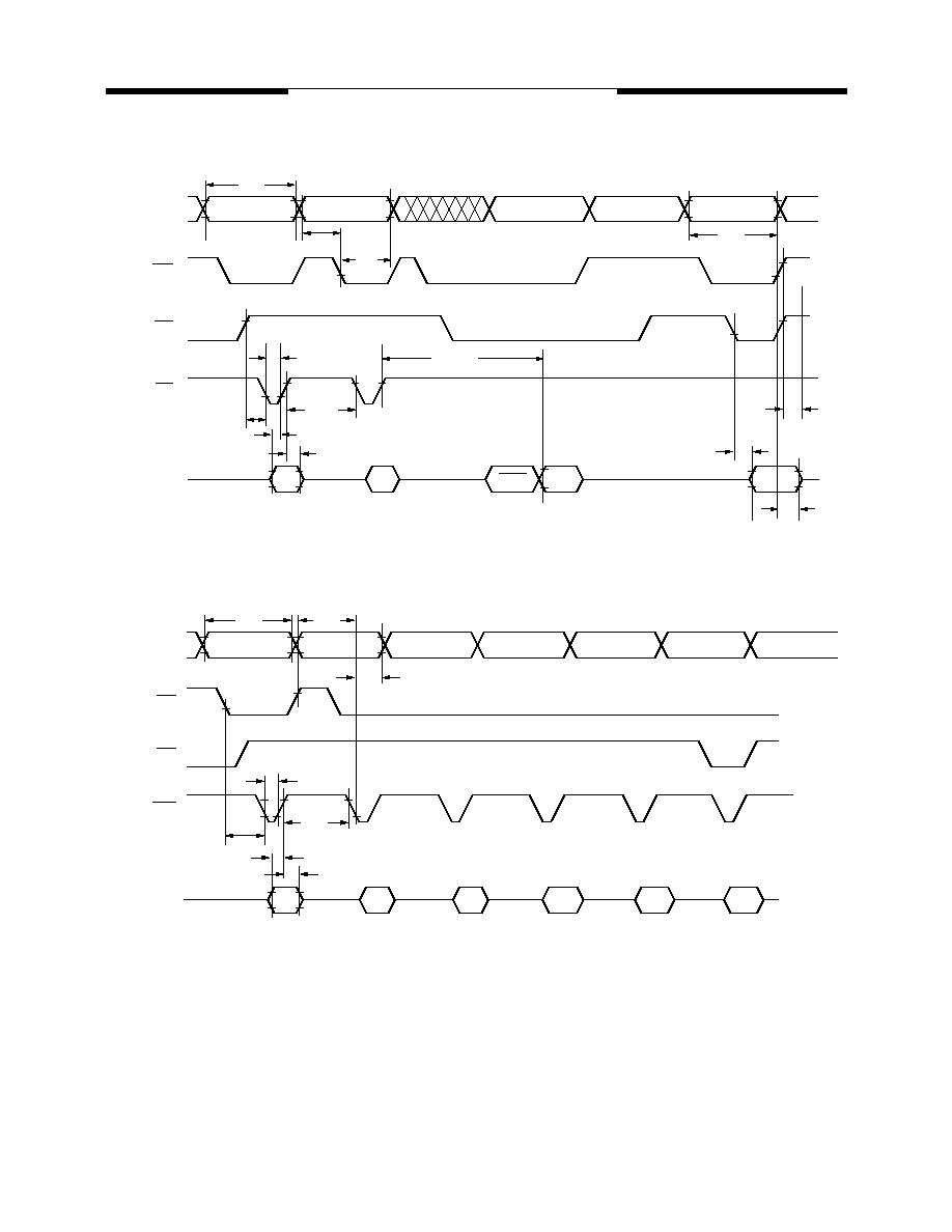
Waveforms of Read Cycle
Waveforms of WE Controlled-Program Cycle
NOTES:
1.
I/O
7
: The output is the complement of the data written to the device.
2.
PA: The address of the memory location to be programmed.
3.
PD: The data at the byte address to be programmed.
t
RC
t
AA
t
CE
t
OE
t
CLZ
t
OH
t
AA
t
OLZ
t
DF
ADDRESS
CE
OE
WE
I/O
VALID DATA OUT
VALID DATA OUT
HIGH-Z
51000-07
HIGH-Z
t
WC
t
AS
PA
5555H
t
WHWH1
t
WPH
t
CS
t
RC
t
AH
t
DS
t
DH
t
WP
t
OES
t
DF
t
OH
t
OE
D
OUT
I/O
7
(1)
PD
(3)
A0H
51000-08
ADDRESS
CE
OE
WE
I/O
3rd bus cycle
PA
(2)
t
CH
MOSEL VITELIC
V29C51000T/V29C51000B
7
V29C51000T/V29C51000B Rev. 0.5 October 2000
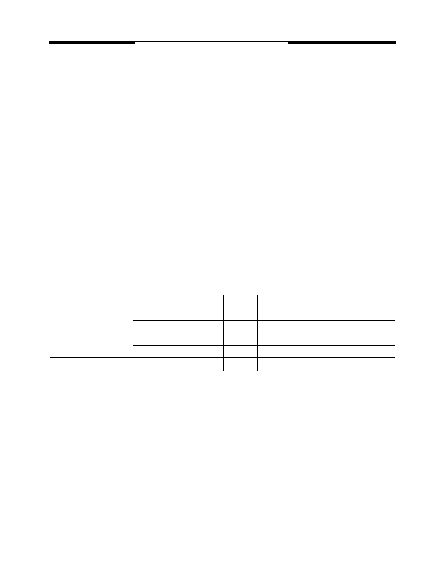
Waveforms of CE Controlled-Program Cycle
Waveforms of Erase Cycle
(1)
NOTES:
1.
PA: The address of the memory location to be programmed.
2.
PD: The data at the byte address to be programmed.
3.
SA: The sector address for Sector Erase. Address = don't care for Chip Erase.
t
WC
t
AS
t
WHWH1
t
WPH
t
OES
t
RC
t
AH
t
DS
t
DH
t
WP
t
DF
t
OH
t
OE
D
OUT
I/O7
PD
(2)
A0H
51000-09
ADDRESS
5555H
PA
PA
(1)
WE
OE
CE
I/O
t
WC
t
AS
t
WPH
ADDRESS
CE
OE
WE
I/O
5555H
5555H
5555H
2AAAH
2AAAH
SA
AAH
55H
80H
AAH
55H
30H
10H for
Chip Erase
51000-10
t
AH
t
WP
t
DS
t
DH
t
CS

8
MOSEL VITELIC
V29C51000T/V29C51000B
V29C51000T/V29C51000B Rev. 0.5 October 2000
Waveforms of DATA Polling Cycle
Waveforms of Toggle Bit Cycle
t
OEH
t
CE
t
WHWH1
t
OH
t
DF
t
CH
CE
OE
WE
I/O
7
I/O
7
I/O
7
VALID DATA OUT
HIGH-Z
t
OE
51000-11
I/O
0
-I/O
6
I/O
0
-I/O
6
INVALID
VALID DATA OUT
HIGH-Z
51000-12
CE
WE
OE
t
OEH
I/O
6

9
V29C51000T/V29C51000B Rev. 0.5 October 2000
MOSEL VITELIC
V29C51000T/V29C51000B
Functional Description
The V29C51000T/V29C51000B consists of 256
equally-sized sectors of 512 bytes each. The 8 KB
lockable Boot Block is intended for storage of the
system BIOS boot code. The boot code is the first
piece of code executed each time the system is
powered on or rebooted.
The V29C51000 is available in two versions: the
V29C51000T with the Boot Block address starting
from E000H to FFFFH, and the V29C51000B with
the Boot Block address starting from 0000H to
FFFFH.
Read Cycle
A read cycle is performed by holding both CE
and OE signals LOW. Data Out becomes valid only
when these conditions are met. During a read cycle
WE must be HIGH prior to CE and OE going LOW.
WE must remain HIGH during the read operation
for the read to complete (see Table 1).
Output Disable
Returning OE or CE HIGH, whichever occurs first
will terminate the read operation and place the l/O
pins in the HIGH-Z state.
Standby
The device will enter standby mode when the CE
signal is HIGH. The l/O pins are placed in the
HIGH-Z, independent of the OE signal.
Command Sequence
T h e V 2 9 C 5 1 0 0 0 T / V 2 9 C 5 1 0 0 0 B d o e s n o t
provide the "reset" feature to return the chip to its
normal state when an incomplete command
sequence or an interruption has happened. In this
case, normal operation (Read Mode) can be
restored by issuing a "non-existent" command
sequence, for example Address: 5555H, Data FFH.
Byte Program Cycle
The V29C51000T/V29C51000B is programmed
on a byte-by-byte basis. The byte program
operation is initiated by using a specific four-bus-
cycle sequence: two unlock program cycles, a
program setup command and program data
program cycles (see Table 2).
During the byte program cycle, addresses are
latched on the falling edge of either CE or WE,
whichever is last. Data is latched on the rising edge
of CE or WE, whichever is first. The byte program
cycle can be CE controlled or WE controlled.
Sector Erase Cycle
The V29C51000T/V29C51000B features a
sector erase operation which allows each sector to
be erased and reprogrammed without affecting
data stored in other sectors. Sector erase operation
is initiated by using a specific six-bus-cycle
sequence: Two unlock program cycles, a setup
command, two additional unlock program cycles,
and the sector erase command (see Table 2). A
sector must be first erased before it can be
reprogrammed. While in the internal erase mode,
8KB Boot Block
512
512
512
512
512
512
8KB Boot Block
V29C51000T
V29C51000B
FFFFH
E000H
0000H
1FFFH
51000-13
0000H
8KB Boot Block = 16 Sectors
Table 1. Operation Modes Decoding
NOTES:
1.
X = Don't Care, V
IH
= HIGH, V
IL
= LOW.
2.
PD: The data at the byte address to be programmed.
Decoding Mode
CE
OE
WE
A
0
A
1
A
9
I/O
Read
V
IL
V
IL
V
IH
A
0
A
1
A
9
READ
Program
V
IL
V
IH
V
IL
A
0
A
1
A
9
PD
Standby
V
IH
X
X
X
X
X
HIGH-Z
Autoselect Device ID
V
IL
V
IL
V
IH
V
IH
V
IL
V
H
CODE
Autoselect Manufacture ID
V
IL
V
IL
V
IH
V
IL
V
IL
V
H
CODE
Output Disable
V
IL
V
IH
V
IH
X
X
X
HIGH-Z
10
MOSEL VITELIC
V29C51000T/V29C51000B
V29C51000T/V29C51000B Rev. 0.5 October 2000
the device ignores any program attempt into the
device. The internal erase completion can be
determined via DATA polling or toggle bit.
The V29C51000T/V29C51000B is shipped with
pre-erased sectors (all bits = 1).
Chip Erase Cycle
The V29C51000T/V29C51000B features a chip-
erase operation. The chip erase operation is
i n i t i a t e d b y u s i n g a s p e c i f i c s i x - b u s - c y c l e
sequence: two unlock program cycles, a setup
command, two additional unlock program cycles,
and the chip erase command (see Table 2).
T h e c h i p e r a s e o p e r a t i o n i s p e r f o r m e d
sequentially, one sector at a time. When the
automated on chip erase algorithm is requested
with the chip erase command sequence, the device
automatically programs and verifies the entire
memory array for an all zero pattern prior to erasure
The automatic erase begins on the rising edge of
the last WE or CE pulse in the command sequence
and terminates when the data on DQ7 is "1".
Program Cycle Status Detection
There are two methods for determining the state
o f t h e V 2 9 C 5 1 0 0 0 T / V 2 9 C 5 1 0 0 0 B d u r i n g a
program (erase/program) cycle: DATA Polling
(I/O
7
) and Toggle Bit (I/O
6
).
DATA Polling (I/O
7
)
The V29C51000T/V29C51000B features DATA
polling to indicate the end of a program cycle.
When the device is in the program cycle, any
attempt to read the device will received the
complement of the loaded data on I/O
7
. Once the
program cycle is completed, I/O
7
will show true
data, and the device is then ready for the next
cycle.
Toggle Bit (I/O
6
)
The V29C51000T/V29C51000B also features
another method for determining the end of a
program cycle. When the device is in the program
cycle, any attempt to read the device will result in
l/O
6
toggling between 1 and 0. Once the program is
completed, the toggling will stop. The device is then
ready for the next operation. Examining the toggle
bit may begin at any time during a program cycle.
Boot Block Protection
T h e V 2 9 C 5 1 0 0 0 T / V 2 9 C 5 1 0 0 0 B f e a t u r e s
hardware Boot Block Protection. This feature will
prevent erasing/programming of data in the Boot
Block once the feature is enabled (see Table 3).
The device is shipped with the Boot Block
unprotected.
Autoselect
The V29C51000T/V29C51000B features an
Autoselect mode to identify the Boot Block
(protected/unprotected), the Device (Top/Bottom),
and the manufacturer ID.
To get to the Autoselect mode, a high voltage
(V
H
) must be applied to the A
9
pin. Once the A
9
signal is returned to LOW or HIGH, the device will
return to the previous mode.
Table 2. Command Codes
NOTES:
1.
Top Boot Sector
2.
Bottom Boot Sector
3.
PA: The address of the memory location to be programmed.
4.
PD: The data at the byte address to be programmed.
Command
Sequence
First Bus
Program Cycle
Second Bus
Program Cycle
Third Bus
Program Cycle
Fourth Bus
Program Cycle
Fifth Bus
Program Cycle
Six Bus
Program Cycle
Address
Data
Address
Data
Address
Data
Address
Data
Address
Data
Address
Data
Read
XXXXH
F0H
Read
5555H
AAH
2AAAH
55H
5555H
F0H
RA
RD
Autoselect
5555H
AAH
2AAAH
55H
5555H
90H
00H
40H
01H
00H
(1)
A0H
(2)
Byte
Program
5555H
AAH
2AAAH
55H
5555H
A0H
PA
PD(4)
Chip Erase
5555H
AAH
2AAAH
55H
5555H
80H
5555H
AAH
2AAAH
55H
5555H
10H
Sector Erase
5555H
AAH
2AAAH
55H
5555H
80H
5555H
AAH
2AAAH
55H
PA(3)
30H
11
V29C51000T/V29C51000B Rev. 0.5 October 2000
MOSEL VITELIC
V29C51000T/V29C51000B
Boot Block Detection
In Autoselect mode, performing a read at
address 3CXX2H or address 0CXX2H will indicate
if the Top Boot Block sector or the Bottom Boot
Block sector is locked out. If the data is 01H, the
Top/Bottom Boot Block is protected. If the data is
00H, the Top/Bottom Boot Block is unprotected.
(see Table 3.)
Device ID
In Autoselect mode, performing a read at
address XXXXH will determine whether the device
is a Top Boot Block device or a Bottom Boot Block
device. If the data is 00H, the device is a Top Boot
Block. If the data is A0H, the device is a Bottom
Boot Block device (see Table 3).
In addition, the device ID can also be read via the
command register when the device is erased or
programmed in a system without applying high
voltage to the A
9
pin. When A
0
is HIGH, the device
ID is presented at the outputs.
Manufacturer ID
In Autoselect mode, performing a read at
address. XXXX0H will determine the manufacturer
ID. 40H is the manufacturer code for Mosel Vitelic
Flash.
In addition the manufacturer ID can also be read
via the command register when the device is
erased or programmed in a system without
applying high voltage to the A
9
pin. when A
0
is
LOW, the manufacturer ID is presented at the
outputs.
Hardware Data Protection
V
CC
Sense Protection: the program operation is
inhibited when VCC is less than 2.5V.
Noise Protection: a CE or WE pulse of less than
5ns will not initiate a program cycle.
Program Inhibit Protection: holding any one of
OE LOW, CE HIGH or WE HIGH inhibits a program
cycle.
Table 3. Autoselect Decoding
NOTE:
1.
X = Don't Care, V
IH
= HIGH, V
IL
= LOW.
Decoding Mode
Boot Block
Address
Data I/O
0
≠I/O
7
A
0
A
1
A
2
≠A
13
A
14
≠A
17
Boot Block Protection
Top
V
IL
V
IH
X
V
IH
01H: protected
Bottom
V
IL
V
IH
X
V
IL
00H: unprotected
Device ID
Top
V
IH
V
IL
X
X
01H
Bottom
00H
Manufacture ID
V
IL
V
IL
X
X
A0H

12
MOSEL VITELIC
V29C51000T/V29C51000B
V29C51000T/V29C51000B Rev. 0.5 October 2000
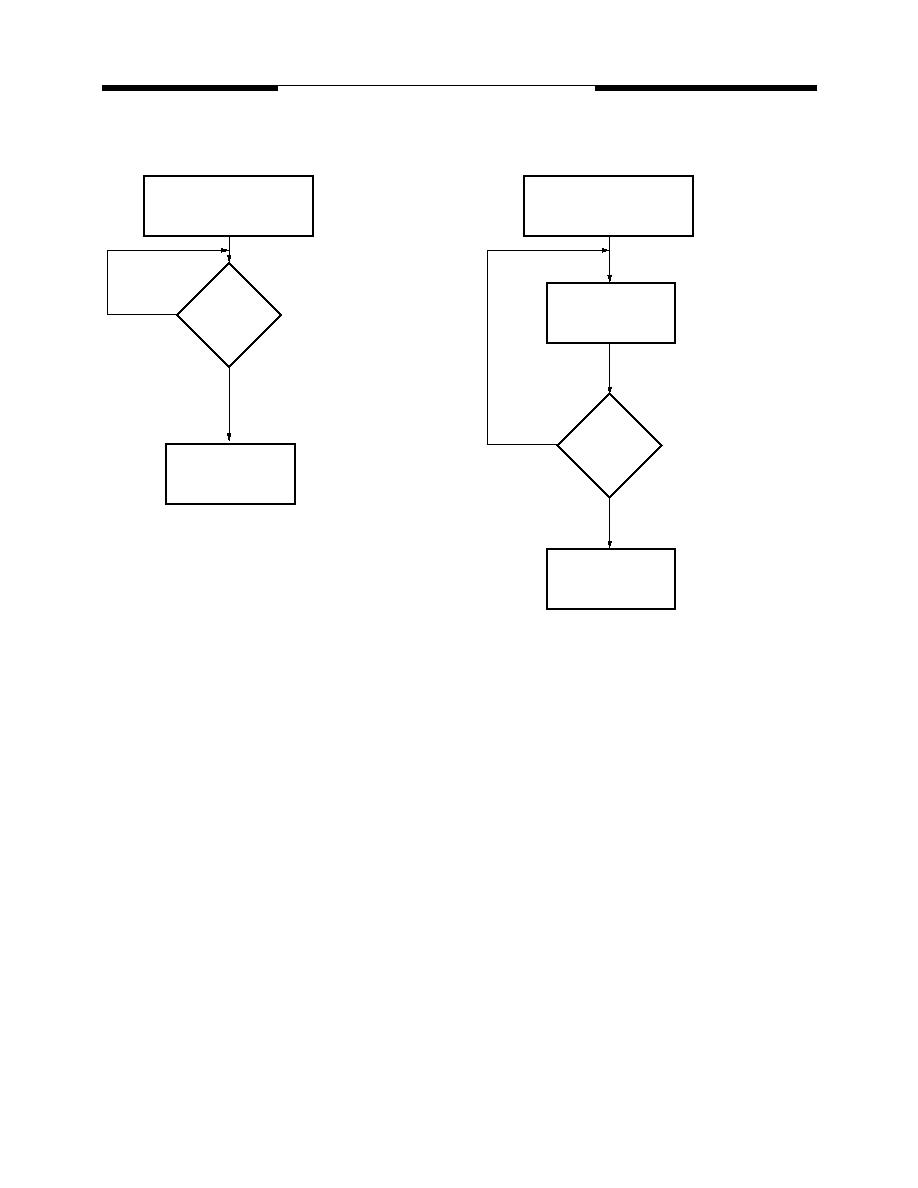
Byte Program Algorithm
Chip/Sector Erase Algorithm
Write Program
Command Sequence
Add/Data
5555H/AAH
2AAAH/55H
5555H/A0H
Four Bus
Cycle
Sequence
PA/PD
DATA
Polling (I/O7)
or Toggle Bit (I/O6)
Programming
Completed
Verify Byte?
Yes
No
Write Erase
Command Sequence
Add/Data
5555H/AAH
2AAAH/55H
5555H/80H
Six Bus
Cycle
Sequence
5555H/AAH
2AAAH/55H
5555H/10H (Chip Erase)
PA/30H (Sector Erase
DATA Polling or Toggle Bit
Successfully Completed
Erase Complete
51000-14
MOSEL VITELIC
V29C51000T/V29C51000B
13
V29C51000T/V29C51000B Rev. 0.5 October 2000
DATA Polling Algorithm
Toggle Bit Algorithm
NOTE:
1.
PBA: The byte address to be programmed.
Read I/O
7
Address = PBA
(1)
Program
Done
Program
Done
I/O
7
= Data
No
Yes
Read I/O
6
No
Yes
I/O
6
Toggle
Read I/O
6
51000-15
14
MOSEL VITELIC
V29C51000T/V29C51000B
V29C51000T/V29C51000B Rev. 0.5 October 2000
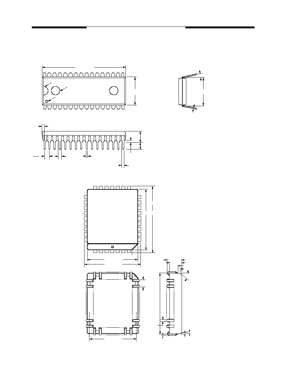
Package Diagrams
32-pin Plastic DIP
32-pin PLCC
15
∞
MAX
0.545/0.555
INDEX-1
.047
+.012
≠ 0
0.210 MAX
0.120 MIN
0.010 MIN
.600 TYP
1.660 MAX.
.050 MAX
.100
TYP
.032 +.012
≠ 0
.018
+.006
≠ .002
.010
+.004
≠ .0004
INDEX-2
EJECTOR MARK
.420
±
.003
3
∞
- 6
∞
3
∞
- 6
∞
3
∞
- 6
∞
.017
30
∞
.136
±
.003
.110
.046
±
.003
.025
.050 TYP
.450
±
.003
.490
±
.005
.045X45
∞
.590
±
.005
.550
±
.003
20
19 18
17 16 15
14
21
22
23
24
25
26
27
28
29
30
31 32
1
2
3
4
13
12
11
10
9
8
7
6
5

MOSEL VITELIC
V29C51000T/V29C51000B
15
V29C51000T/V29C51000B Rev. 0.5 October 2000
32-pin TSOP-I
0.032 TYP.
0.020 SBC
0.003 MAX
0.020 MAX.
0.024
±
0.004
SEATING
PLANE
0.010
See Detail "A"
Detail "A"
0.724 TYP. (0.728 MAX.)
0.787
±
0.008
0.009
±
0.002
0.315 TYP.
(0.319 MAX.)
0.035
±
0.002
0.047 MAX.
0.005 MIN.
0.007 MAX.
Units in inches

MOSEL VITELIC
WORLDWIDE OFFICES
V29C51000T/V29C51000B
MOSEL VITELIC
3910 N. First Street, San Jose, CA 95134-1501 Ph: (408) 433-6000 Fax: (408) 433-0952 Tlx: 371-9461
The information in this document is subject to change without
notice.
MOSEL VITELIC makes no commitment to update or keep cur-
rent the information contained in this document. No part of this
document may be copied or reproduced in any form or by any
means without the prior written consent of MOSEL-VITELIC.
MOSEL VITELIC subjects its products to normal quality control
sampling techniques which are intended to provide an assurance
of high quality products suitable for usual commercial applica-
tions. MOSEL VITELIC does not do testing appropriate to provide
100% product quality assurance and does not assume any liabil-
ity for consequential or incidental arising from any use of its prod-
ucts. If such products are to be used in applications in which
personal injury might occur from failure, purchaser must do its
own quality assurance testing appropriate to such applications.
© Copyright 2000, MOSEL VITELIC Inc.
10/00
Printed in U.S.A.
U.S. SALES OFFICES
U.S.A.
3910 NORTH FIRST STREET
SAN JOSE, CA 95134
PHONE: 408-433-6000
FAX: 408-433-0952
HONG KONG
19 DAI FU STREET
TAIPO INDUSTRIAL ESTATE
TAIPO, NT, HONG KONG
PHONE: 852-2666-3307
FAX: 852-2770-8011
TAIWAN
7F, NO. 102
MIN-CHUAN E. ROAD, SEC. 3
TAIPEI
PHONE: 886-2-2545-1213
FAX: 886-2-2545-1209
NO 19 LI HSIN ROAD
SCIENCE BASED IND. PARK
HSIN CHU, TAIWAN, R.O.C.
PHONE: 886-3-579-5888
FAX: 886-3-566-5888
SINGAPORE
10 ANSON ROAD #23-13
INTERNATIONAL PLAZA
SINGAPORE 079903
PHONE: 65-3231801
FAX: 65-3237013
JAPAN
ONZE 1852 BUILDING 6F
2-14-6 SHINTOMI, CHUO-KU
TOKYO 104-0041
PHONE: 03-3537-1400
FAX: 03-3537-1402
UK & IRELAND
SUITE 50, GROVEWOOD
BUSINESS CENTRE
STRATHCLYDE BUSINESS
PARK
BELLSHILL, LANARKSHIRE,
SCOTLAND, ML4 3NQ
PHONE: 44-1698-748515
FAX: 44-1698-748516
GERMANY
(CONTINENTAL
EUROPE & ISRAEL)
BENZSTRASSE 32
71083 HERRENBERG
GERMANY
PHONE: +49 7032 2796-0
FAX: +49 7032 2796 22
NORTHWESTERN
3910 NORTH FIRST STREET
SAN JOSE, CA 95134
PHONE: 408-433-6000
FAX: 408-433-0952
SOUTHWESTERN
302 N. EL CAMINO REAL #200
SAN CLEMENTE, CA 92672
PHONE: 949-361-7873
FAX: 949-361-7807
CENTRAL,
NORTHEASTERN &
SOUTHEASTERN
604 FIELDWOOD CIRCLE
RICHARDSON, TX 75081
PHONE: 972-690-1402
FAX: 972-690-0341