MOSEL VITELIC
1
V53C316405A
3.3 VOLT 4M x 4 EDO PAGE MODE
CMOS DYNAMIC RAM
V53C316405A Rev. 1.2 March 1998
V53C316405A
50
60
Max. RAS Access Time, (t
RAC
)
50 ns
60 ns
Max. Column Address Access Time, (t
CAA
)
25 ns
30 ns
Min. Extended Data Out Page Mode Cycle Time, (t
PC
)
20 ns
25 ns
Min. Read/Write Cycle Time, (t
RC
)
84 ns
104 ns
Features
s
4M x 4-bit organization
s
EDO Page Mode for a sustained data rate
of 50 MHz
s
RAS access time: 50, 60 ns
s
Low power dissipation
s
Read-Modify-Write, RAS-Only Refresh,
CAS-Before-RAS Refresh and Hidden Refresh
s
Refresh Interval: 4096 cycles/64 ms
s
Available in 24/26-pin 300 mil SOJ,
and 24/26-pin 300 mil TSOP-II
s
Single +3.3V
±
0.3V Power Supply
s
TTL Interface
Description
The V53C316405A is a 4,194,304 x 4 bit high-
performance CMOS dynamic random access mem-
ory. The V53C316405A offers Page mode opera-
tion with Extended Data Output. The V53C316405A
has asymmetric address, 12-bit row and 10-bit col-
umn.
All inputs are TTL compatible. EDO Page Mode
operation allows random access up to 1024 x 4 bits,
within a page, with cycle times as short as 20ns.
These features make the V53C316405A ideally
suited for a wide variety of high performance com-
puter systems and peripheral applications.
Device Usage Chart
Operating
Temperature
Range
Package Outline
Access Time (ns)
Power
Temperature
Mark
K
T
50
60
Std.
0
∞
C to 70
∞
C
∑
∑
∑
∑
∑
Blank
2
MOSEL VITELIC
V53C316405A
V53C316405A Rev. 1.2 March 1998
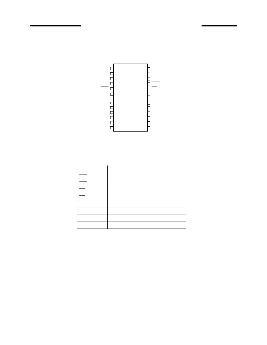
Pin Names
A
0
≠A
11
Row, Column Address Inputs
RAS
Row Address Strobe
CAS
Column Address Strobe
WE
Write Enable
OE
Output Enable
I/O
1
≠I/O
4
Data Input, Output
V
CC
+3.3V Supply
V
SS
0V Supply
NC
No Connect
24/26-Pin Plastic SOJ/TSOP-II
PIN CONFIGURATION
Top View
WE
RAS
I/O1
I/O2
A 0
A1
A2
A3
VCC
VCC
1
2
3
4
5
9
10
11
12
13
26
25
24
23
22
18
17
16
15
14
V
I/O
I/O
CAS
OE
A
A
A
A
V
SS
4
3
7
A10
311640500-02
19
A 8
9
6
5
4
SS
6
21
A
A11
3
MOSEL VITELIC
V53C316405A
V53C316405A Rev. 1.2 March 1998
Absolute Maximum Ratings*
Operating temperature range ..................0 to 70
∞
C
Storage temperature range ............... -55 to 150
∞
C
Input/output voltage .... -0.5 to min (V
CC
+0.5, 4.6) V
Power supply voltage .......................... -1.0 to 4.6 V
Power dissipation .......................................... 0.5 W
Data out current (short circuit) ...................... 50 mA
*Note:
Operation above Absolute Maximum Ratings can
adversely affect device reliability.
Capacitance*
T
A
= 25
∞
C, V
CC
= 3.3 V
±
0.3V, V
SS
= 0 V
*Note:
Capacitance is sampled and not 100% tested.
Symbol
Parameter
Typ.
Max.
Unit
C
IN1
Address Input
--
5
pF
C
IN2
RAS, CAS, WE, OE
--
7
pF
C
OUT
Data Input/Output
--
7
pF
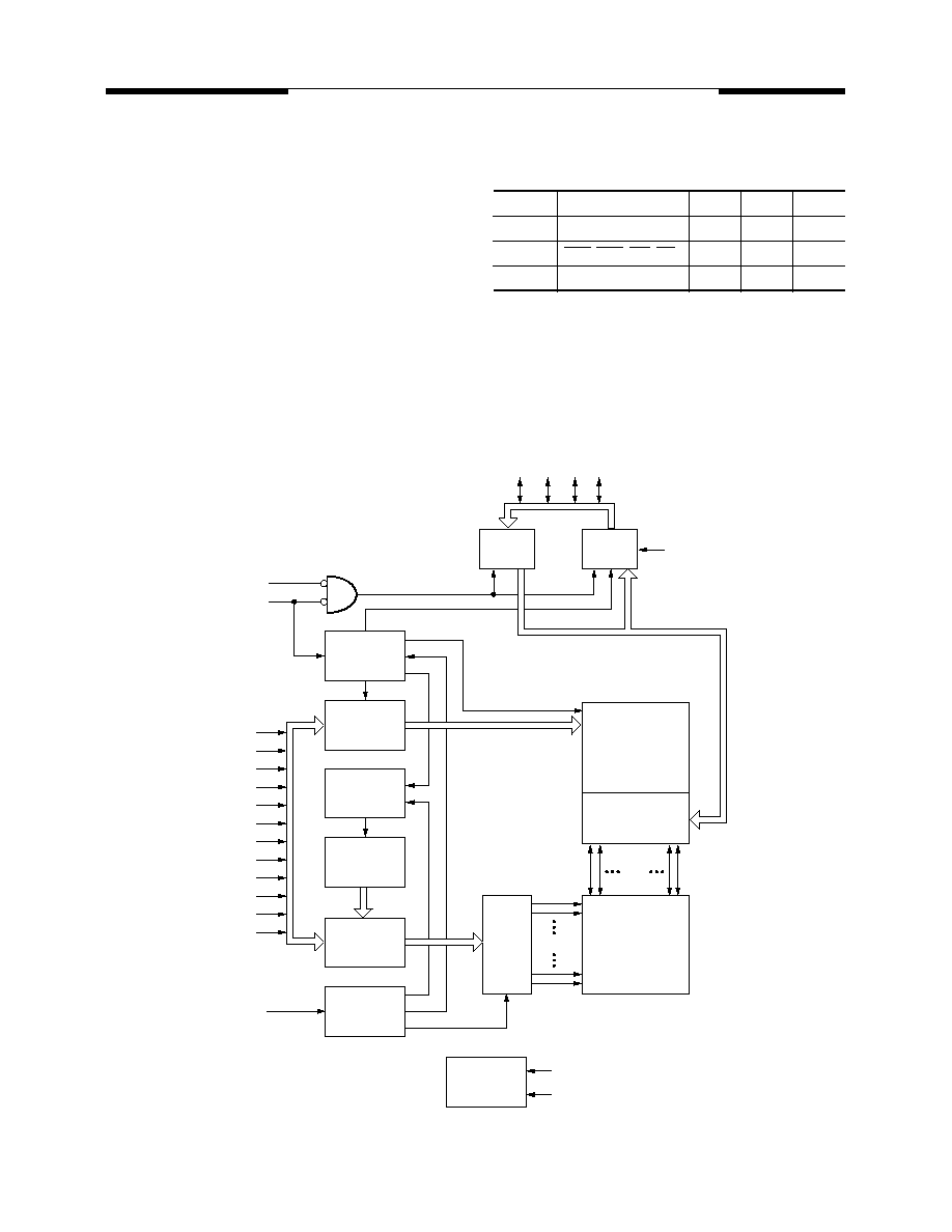
Block Diagram
No. 2 Clock
Generator
Data In
Buffer
Data Out
Buffer
Column
Address
Buffers (10)
Refresh
Controller
Row
Decoder
Refresh
Counter (12)
No. 1 Clock
Generator
Voltage Down
Generator
Row
Address
Buffers (11)
10
4
I/O1 I/O2 I/O3 I/O4
4
OE
12
12
12
4
4096
VCC
VCC (internal)
1024
x4
Memory Array
4096 x 1024 x 4
Sense Amplifier
I/O Gating
Column
Decoder
A0
CAS
WE
A1
A2
A3
A4
A5
A6
A7
A8
A9
A10
A11
RAS
10
311640502-04
4096 x 4
4
V53C316405A Rev. 1.2 March 1998
MOSEL VITELIC
V53C316405A
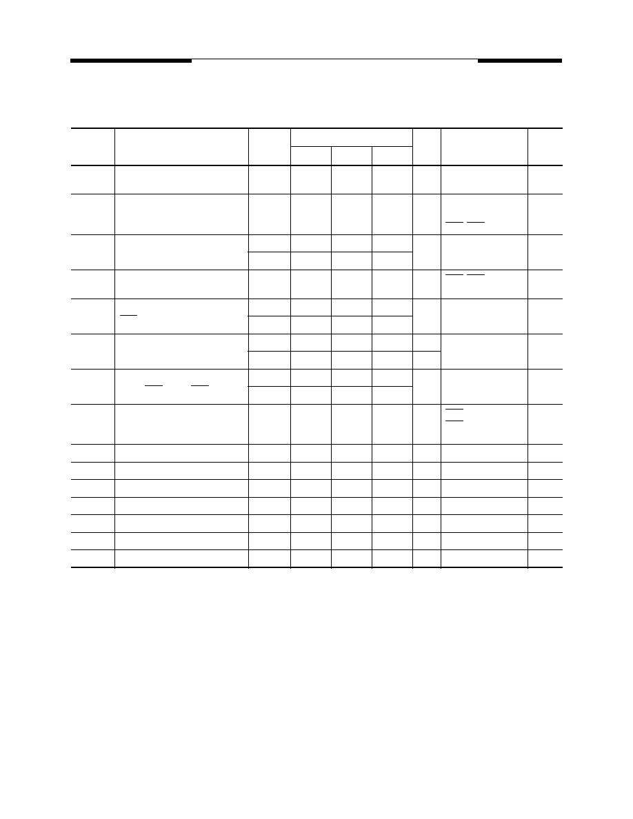
DC and Operating Characteristics
(1-2)
T
A
= 0
∞
C to 70
∞
C, V
CC
= 3.3 V
±
0.3V, V
SS
= 0 V, V
T
= 2ns unless otherwise specified.
Symbol
Parameter
Access
Time
V53C316405A
Unit
Test Conditions
Notes
Min.
Typ.
Max.
I
LI
Input Leakage Current
(any input pin)
≠10
10
µ
A
V
SS
V
IN
V
CC
+0.3V
1
I
LO
Output Leakage Current
(for High-Z State)
≠10
10
µ
A
V
SS
V
OUT
V
CC
+0.3V
RAS, CAS at V
IH
1
I
CC1
V
CC
Supply Current,
Operating
50
50
mA
t
RC
= t
RC
(min.)
2, 3, 4
60
40
I
CC2
V
CC
Supply Current,
TTL Standby
2
mA
RAS, CAS at V
IH
other inputs
V
SS
I
CC3
V
CC
Supply Current,
RAS-Only Refresh
50
50
mA
t
RC
= t
RC
(min.)
2, 4
60
40
I
CC4
V
CC
Supply Current,
EDO Page Mode Operation
50
35
mA
Minimum Cycle
2, 3, 4
60
30
I
CC5
V
CC
Supply Current,
during CAS-before-RAS Refresh
50
50
mA
2, 4
60
40
I
CC6
V
CC
Supply Current,
CMOS Standby
1.0
mA
RAS
V
CC
≠ 0.2 V,
CAS
V
CC
≠ 0.2 V,
other input pins
V
SS
1
V
CC
Power Supply Voltage
3.0
3.3
3.6
V
V
IL
Input Low Voltage
≠0.5
0.8
V
1
V
IH
Input High Voltage
2.0
V
CC
+ 0.5
V
1
V
OL
TTL Output Low Voltage
0.4
V
I
OL
= 2 mA
1
V
OH
TTL Output High Voltage
2.4
V
I
OH
= ≠2 mA
1
V
OL
CMOS Output Low Voltage
0.2
V
I
OL
= 100
µ
A
1
V
OH
CMOS Output High Voltage
V
CC
≠ 0.2
V
I
OH
= ≠100
µ
A
1
5
MOSEL VITELIC
V53C316405A
V53C316405A Rev. 1.2 March 1998
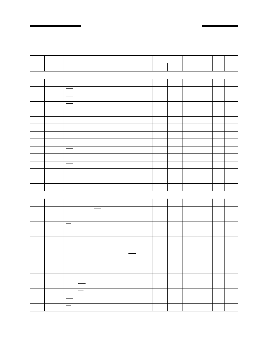
AC Characteristics
(5,6)
T
A
= 0 to 70 ∞C,V
CC
= 3.3 V
±
0.3V, t
T
= 2 ns
#
Symbol
Parameter
-50
-60
Unit
Note
min.
max.
min.
max.
Common Parameters
1
t
RC
Random read or write cycle time
84
≠
104
≠
ns
2
t
RP
RAS precharge time
30
≠
40
≠
ns
3
t
RAS
RAS pulse width
50
10k
60
10k
ns
4
t
CAS
CAS pulse width
8
10k
10
10k
ns
5
t
ASR
Row address setup time
0
≠
0
≠
ns
6
t
RAH
Row address hold time
8
≠
10
≠
ns
7
t
ASC
Column address setup time
0
≠
0
≠
ns
8
t
CAH
Column address hold time
8
≠
10
≠
ns
9
t
RCD
RAS to CAS delay time
12
37
14
45
ns
10
t
RAD
RAS to column address delay
10
25
12
30
ns
11
t
RSH
RAS hold time
13
15
≠
ns
12
t
CSH
CAS hold time
40
50
≠
ns
13
t
CRP
CAS to RAS precharge time
5
≠
5
≠
ns
14
t
T
Transition time (rise and fall)
1
50
1
50
ns
7
15
t
REF
Refresh period
≠
64
≠
64
ms
Read Cycle
16
t
RAC
Access time from RAS
≠
50
≠
60
ns
8, 9
17
t
CAC
Access time from CAS
≠
13
≠
15
ns
8, 9
18
t
CAA
Access time from column address
≠
25
≠
30
ns
8,10
19
t
OEA
OE access time
≠
13
≠
15
ns
20
t
RAL
Column address to RAS lead time
25
≠
30
≠
ns
21
t
RCS
Read command setup time
0
≠
0
≠
ns
22
t
RCH
Read command hold time
0
≠
0
≠
ns
11
23
t
RRH
Read command hold time referenced to RAS
0
≠
0
≠
ns
11
24
t
CLZ
CAS to output in low-Z
0
≠
0
≠
ns
8
25
t
OFF
Output buffer turn-off delay
0
13
0
15
ns
12
26
t
OEZ
Output turn-off delay from OE
0
13
0
15
ns
12
27
t
DZC
Data to CAS low delay
0
≠
0
≠
ns
13
28
t
DZO
Data to OE low delay
0
≠
0
≠
ns
13
29
t
CDD
CAS high to data delay
10
≠
13
≠
ns
14
30
t
ODD
OE high to data delay
10
≠
13
≠
ns
14