
MOSEL VITELIC
1
V53C518165A
1M x 16 EDO PAGE MODE
CMOS DYNAMIC RAM
OPTIONAL SELF REFRESH
V53C518165A Rev. 1.1 January 1998
HIGH PERFORMANCE
50
60
Max. RAS Access Time, (t
RAC
)
50 ns
60 ns
Max. Column Address Access Time, (t
CAA
)
25 ns
30 ns
Min. Extended Data Out Page Mode Cycle Time, (t
PC
)
20 ns
25 ns
Min. Read/Write Cycle Time, (t
RC
)
84 ns
104 ns
Features
s
1MB x 16-bit organization
s
EDO Page Mode for a sustained data rate
of 50 MHz
s
RAS access time: 50, 60 ns
s
Dual CAS Inputs
s
Low power dissipation
s
Read-Modify-Write, RAS-Only Refresh,
CAS-Before-RAS Refresh
� Refresh Interval: 1024 cycles/16 ms
s
Available in 42-pin 400 mil SOJ and
44/50-pin 400 mil TSOP-II Packages
s
Single 5V
�
10% Power Supply
s
TTL Interface
s
Optional Self Refresh (V53C518165AS)
� Refresh Interval: 1024 cycles/128 ms
Description
The V53C518165A is a 1048576 x 16 bit high-
performance CMOS dynamic random access
memory. The V53C518165A offers Page mode op-
e r a t i o n w i t h E x t e n d e d D a t a O u t p u t . T h e
V53C518165A has symmetric address, 10-bit row
and 10-bit column.
All inputs are TTL compatible. EDO Page Mode
operation allows random access up to 1024 x 16
bits, within a page, with cycle times as short as
20ns.
These features make the V53C518165A ideally
suited for a wide variety of high performance com-
puter systems and peripheral applications.
Device Usage Chart
Operating
Temperature
Range
Package Outline
Access Time (ns)
Power
Temperature
Mark
K
T
50
60
Std.
0
�
C to 70
�
C
�
�
�
�
�
Blank
�40
�
C to +85
�
C
�
�
�
�
�
I
2
V53C518165A Rev. 1.1 January 1998
MOSEL VITELIC
V53C518165A
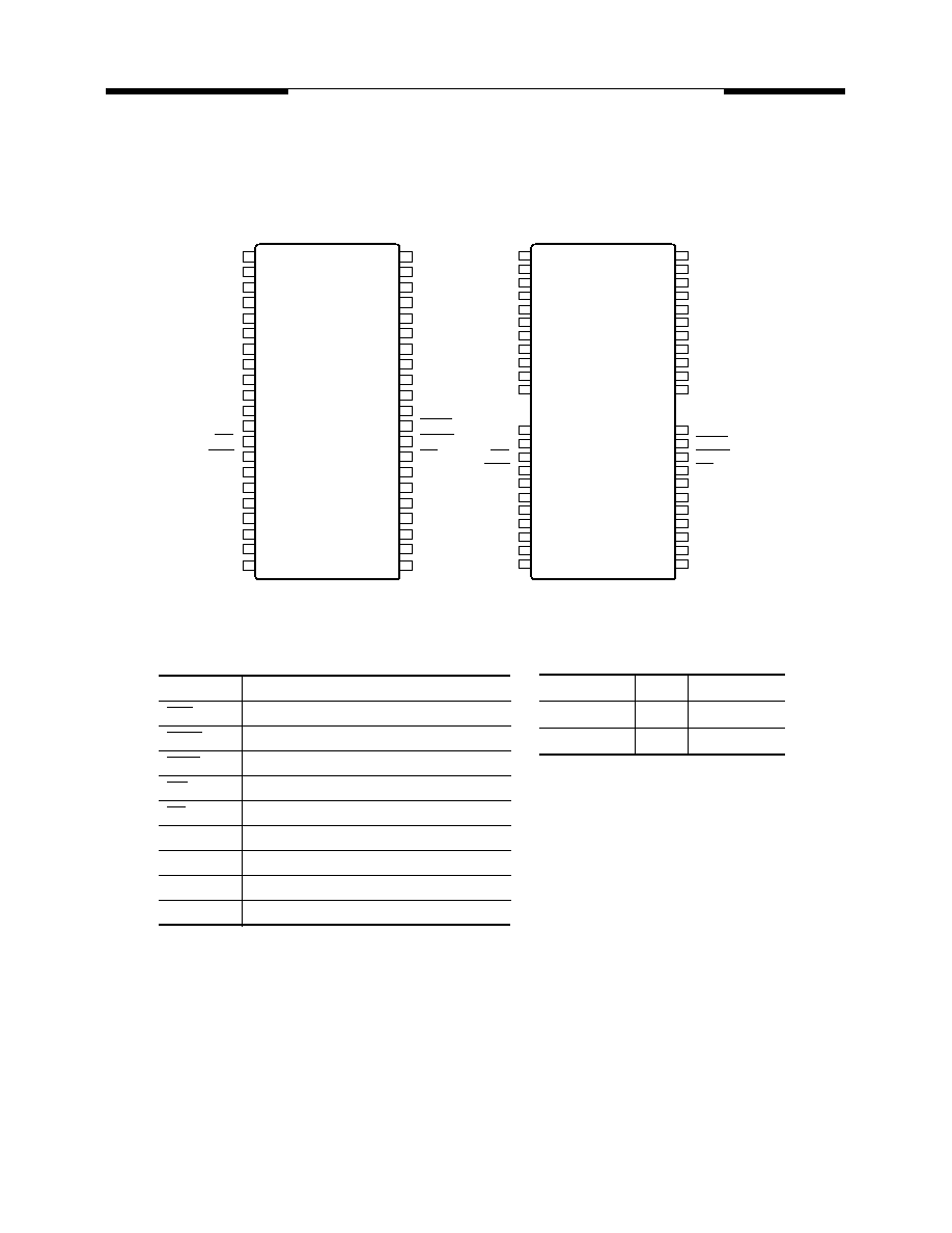
Pin Names
A
0
�A
9
Row, Column Address Inputs
RAS
Row Address Strobe
UCAS
Column Address Strobe/Upper Byte Control
LCAS
Column Address Strobe/Lower Byte Control
WE
Write Enable
OE
Output Enable
I/O
1
�I/O
16
Data Input, Output
V
CC
+5V Supply
V
SS
0V Supply
NC
No Connect
Description
Pkg.
Pin Count
TSOP-II
T
44/50
SOJ
K
42
V
CC
I/O
1
I/O
2
I/O
3
I/O
4
VCC
I/O
5
I/O
6
I/O
7
I/O
8
NC
NC
WE
RAS
NC
NC
A0
A
1
A
2
A
3
V
CC
V
SS
I/O
16
I/O
15
I/O
14
I/O
13
V
SS
I/O
12
I/O
11
I/O
10
I/O
9
NC
LCAS
UCAS
OE
A
9
A
8
A
7
A
6
A
5
A
4
V
SS
5
6
7
8
9
10
11
12
1
2
3
4
40
39
38
37
36
35
34
33
32
31
30
29
13
14
15
16
17
18
19
20
28
27
26
25
24
23
22
42
21
41
V
CC
I/O
1
I/O
2
I/O
3
I/O
4
VCC
I/O
5
I/O
6
I/O
7
I/O
8
NC
NC
NC
WE
RAS
NC
NC
A0
A
1
A
2
A
3
V
CC
V
SS
I/O
16
I/O
15
I/O
14
I/O
13
V
SS
I/O
12
I/O
11
I/O
10
I/O
9
NC
NC
LCAS
UCAS
OE
A
9
A
8
A
7
A
6
A
5
A
4
V
SS
5
6
7
8
9
10
11
1
2
3
4
15
16
17
18
19
20
511816500-02
21
22
23
24
25
46
45
44
43
42
41
40
50
49
48
47
36
35
34
33
32
31
30
29
28
27
26
42-Pin Plastic SOJ
PIN CONFIGURATION
Top View
44/50-Pin Plastic TSOP-II
PIN CONFIGURATION
Top View
3
V53C518165A Rev. 1.1 January 1998
MOSEL VITELIC
V53C518165A
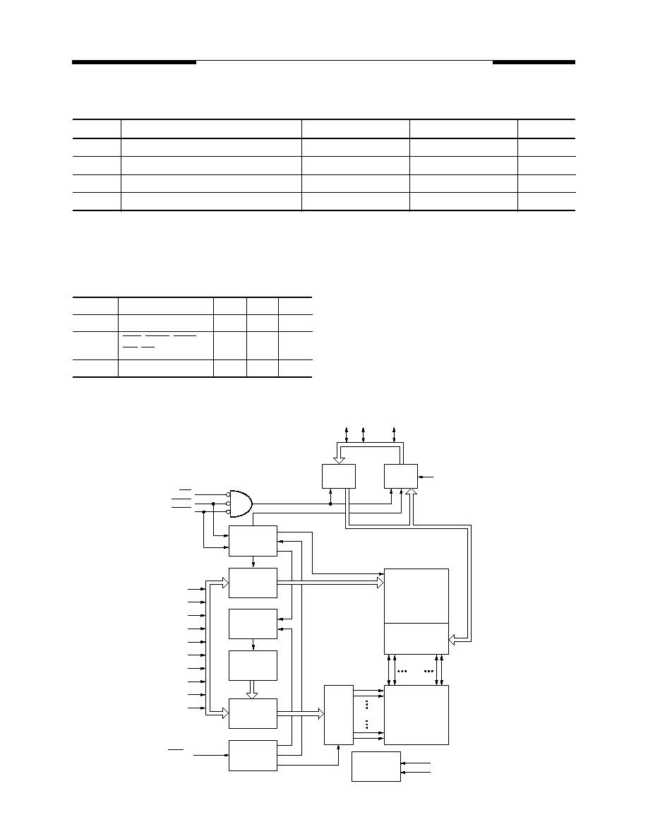
Block Diagram
No. 2 Clock
Generator
Data In
Buffer
Data Out
Buffer
Column
Address
Buffers (10)
Refresh
Controller
Row
Decoder
Refresh
Counter (10)
Voltage Down
Generator
No. 1 Clock
Generator
Row
Address
Buffers (10)
10
16
I/O1 I/O2
I/O16
16
VCC
VCC (internal)
OE
10
10
10
16
1024
1024
x16
Memory Array
1024 x 1024 x 16
Sense Amplifier
I/O Gating
316516500-03
Column
Decoder
A0
UCAS
WE
LCAS
A1
A2
A3
A4
A5
A6
A7
A8
A9
RAS
10
� � �
Absolute Maximum Ratings*
*
Note:
Stresses greater than those listed under "Absolute Maximum Ratings" may cause permanent damage to the device. This is a
stress rating only and functional operation of the device at these or any other conditions above those indicated in the operational
sections of this specification is not implied. Exposure to absolute maximum rating conditions for extended periods may affect
reliability.
Capacitance*
T
A
= 25
�
C, V
CC
= 5 V
�
10%, V
SS
= 0 V, f = 1 MHz
*
Note:
Capacitance is sampled and not 100% tested.
Symbol
Parameter
Commercial
Extended
Units
V
N
Power Supply Voltage
-1 to +7
-1 to +7
V
V
DQ
Input/Output Voltage
-0.5 to min (V
CC
+0.5, 7.0)
-0.5 to min (V
CC
+0.5, 7.0)
V
T
BIAS
Temperature Under Bias
-10 to +125
-65 to +135
�
C
T
STG
Storage Temperature
-55 to +125
-65 to +150
�
C
Symbol
Parameter
Min.
Max.
Unit
C
IN1
Address Input
--
5
pF
C
IN2
RAS, UCAS, LCAS,
WE, OE
--
7
pF
C
OUT
Data Input/Output
--
7
pF
4
V53C518165A Rev. 1.1 January 1998
MOSEL VITELIC
V53C518165A
DC and Operating Characteristics
(1-2)
T
A
= 0
�
C to 70
�
C, V
CC
= 5 V
�
10%, V
SS
= 0 V, t
T
= 2ns, unless otherwise specified.
Symbol
Parameter
Access
Time
Commercial
Extended
Unit
Test Conditions
Notes
Min.
Max.
Min.
Max.
I
LI
Input Leakage Current
(any input pin)
�10
10
�10
10
m
A
V
SS
�
V
IN
�
V
CC
+
0.5V
1
I
LO
Output Leakage Current
(for High-Z State)
�10
10
�10
10
m
A
V
SS
�
V
OUT
�
V
CC
+
0.5V
RAS, CAS at V
IH
1
I
CC1
V
CC
Supply Current,
Operating
50
130
200
mA
t
RC
= t
RC
(min.)
2, 3, 4
60
115
180
I
CC2
V
CC
Supply Current,
TTL Standby
2
2
mA
RAS, CAS at V
IH
other inputs
�
V
SS
I
CC3
V
CC
Supply Current,
RAS-Only Refresh
50
130
200
mA
t
RC
= t
RC
(min.)
2, 4
60
115
180
I
CC4
V
CC
Supply Current,
EDO Page Mode
Operation
50
50
90
mA
Minimum Cycle
2, 3, 4
60
40
75
I
CC5
V
CC
Supply Current,
during CAS-before-RAS Refresh
50
130
200
mA
t
RC
= t
RC
(min.)
2, 4
60
115
180
I
CC6
V
CC
Supply Current,
CMOS Standby
1.0
1.0
mA
RAS
�
V
CC
� 0.2 V,
CAS
�
V
CC
� 0.2 V
other input
�
V
SS
1
I
CC7
Self Refresh (Optional)
250
250
m
A
CBR cycle with
t
RAS
�
t
RASS (min.)
,
CAS Held Low,
WE = V
CC
-0.2V,
Address and
D
IN
= V
CC
-0.2V or
0.2V
V
CC
Power Supply Voltage
4.5
5.5
4.5
5.5
V
V
IL
Input Low Voltage
�0.5
0.8
�0.5
0.8
V
1
V
IH
Input High Voltage
2.4
V
CC
+0.5
2.4
V
CC
+0.5
V
1
V
OL
Output Low Voltage
0.4
0.4
V
I
OL
= 4.2 mA
1
V
OH
Output High Voltage
2.4
2.4
V
I
OH
= �5.0 mA
1

5
V53C518165A Rev. 1.1 January 1998
MOSEL VITELIC
V53C518165A
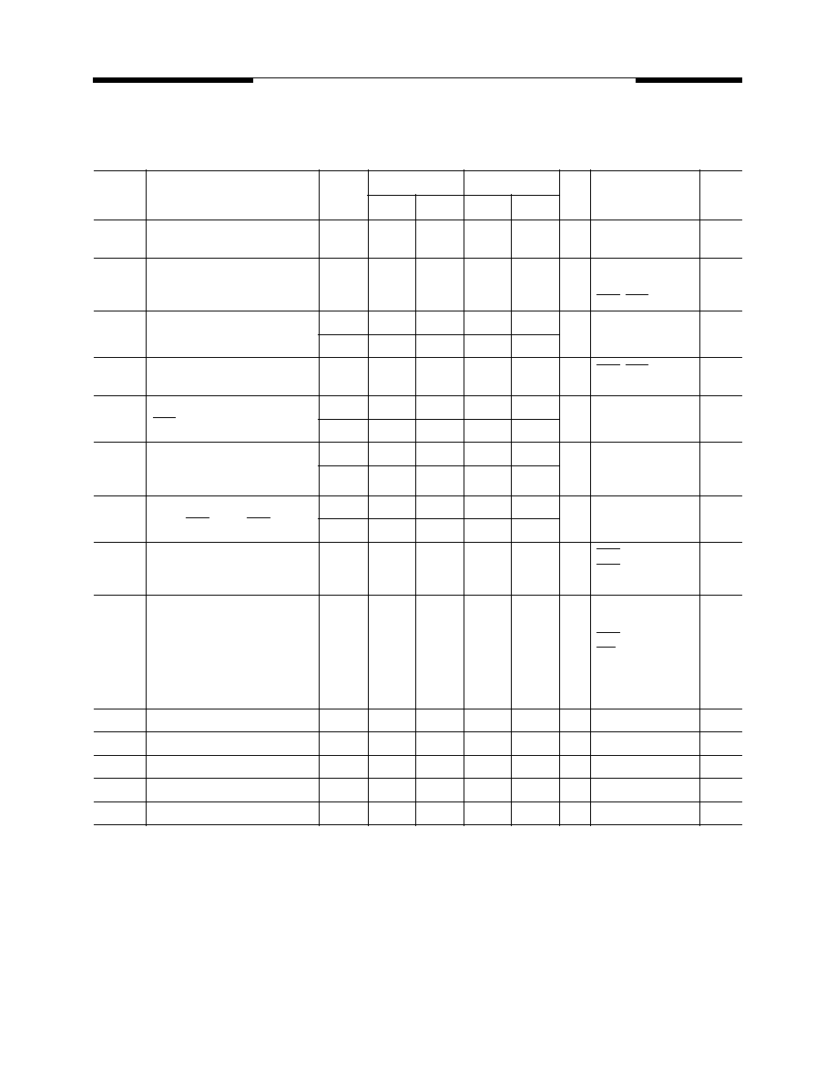
AC Characteristics
(5,6)
T
A
= 0
�
C to 70
�
C, V
CC
= 5 V
�
10%, t
T
= 2ns, unless otherwise noted
#
Symbol
Parameter
Limit Values
Unit
Note
-50
-60
Min.
Max.
Min.
Max.
Common Parameters
1
t
RC
Random read or write cycle time
84
--
104
--
ns
2
t
RP
RAS precharge time
30
--
40
--
ns
3
t
RAS
RAS pulse width
50
10k
60
10k
ns
4
t
CAS
CAS pulse width
8
10k
10
10k
ns
5
t
ASR
Row address setup time
0
--
0
--
ns
6
t
RAH
Row address hold time
8
--
10
--
ns
7
t
ASC
Column address setup time
0
--
0
--
ns
8
t
CAH
Column address hold time
8
--
10
--
ns
9
t
RCD
RAS to CAS delay time
12
37
14
45
ns
10
t
RAD
RAS to column address delay
10
25
12
30
ns
11
t
RSH
RAS hold time
13
--
15
--
ns
12
t
CSH
CAS hold time
40
--
50
--
ns
13
t
CRP
CAS to RAS precharge time
5
--
5
--
ns
14
t
T
Transition time (rise and fall)
1
50
1
50
ns
7
15
t
REF
Refresh period
--
16
--
16
ms
Read Cycle
16
t
RAC
Access time from RAS
--
50
--
60
ns
8, 9
17
t
CAC
Access time from CAS
--
13
--
15
ns
8, 9
18
t
CAA
Access time from column address
--
25
--
30
ns
8,10
19
t
OAC
OE access time
--
13
--
15
ns
20
t
CAR
Column address to RAS lead time
25
--
30
--
ns
21
t
RCS
Read command setup time
0
--
0
--
ns
22
t
RCH
Read command hold time
0
--
0
--
ns
11
23
t
RRH
Read command hold time referenced to RAS
0
--
0
--
ns
11
24
t
CLZ
CAS to output in low-Z
0
--
0
--
ns
8
25
t
OFF
Output buffer turn-off delay
0
13
0
15
ns
12
26
t
OEZ
Output turn-off delay from OE
0
13
0
15
ns
12
27
t
DZC
Data to CAS low delay
0
--
0
--
ns
13
28
t
DZO
Data to OE low delay
0
--
0
--
ns
13
29
t
CDD
CAS high to data delay
10
--
13
--
ns
14
30
t
ODD
OE high to data delay
10
--
13
--
ns
14