MOSEL VITELIC
1
V54C3128(16/80/40)4V(BGA)
128Mbit SDRAM
3.3 VOLT, BGA PACKAGE
8M X 16
16M X 8
32M X 4
V54C3128(16/80/40)4V(BGA) Rev. 1.3 November 2002
PRELIMINARY
6
7PC
7
8PC
System Frequency (f
CK
)
166 MHz
143 MHz
143 MHz
125 MHz
Clock Cycle Time (t
CK3
)
6 ns
7 ns
7 ns
8 ns
Clock Access Time (t
AC3
) CAS Latency = 3
5.4 ns
5.4 ns
5.4 ns
6 ns
Clock Access Time (t
AC2
) CAS Latency = 2
5.4 ns
5.4 ns
6 ns
6 ns
Features
4 banks x 2Mbit x 16 organization
4 banks x 4Mbit x 8 organization
4 banks x 8Mbit x 4 organization
High speed data transfer rates up to 166 MHz
Full Synchronous Dynamic RAM, with all signals
referenced to clock rising edge
Single Pulsed RAS Interface
Data Mask for Read/Write Control
Four Banks controlled by BA0 & BA1
Programmable CAS Latency: 2, 3
Programmable Wrap Sequence: Sequential or
Interleave
Programmable Burst Length:
1, 2, 4, 8 for Sequential Type
1, 2, 4, 8 for Interleave Type
Multiple Burst Read with Single Write Operation
Automatic and Controlled Precharge Command
Random Column Address every CLK (1-N Rule)
Power Down Mode
Auto Refresh and Self Refresh
Refresh Interval: 4096 cycles/64 ms
Available in 60 Pin WBGA
LVTTL Interface
Single +3.3 V
�
0.3 V Power Supply
Description
The V54C3128(16/80/40)4V(BGA) is a four bank
Synchronous DRAM organized as 4 banks x 2Mbit
x 16, 4 banks x 4Mbit x 8, or 4 banks x 8Mbit x 4.
The V54C3128(16/80/40)4V(BGA) achieves high
speed data transfer rates up to 166 MHz by employ-
ing a chip architecture that prefetches multiple bits
and then synchronizes the output data to a system
clock
All of the control, address, data input and output
circuits are synchronized with the positive edge of
an externally supplied clock.
Operating the four memory banks in an inter-
leaved fashion allows random access operation to
occur at higher rate than is possible with standard
DRAMs. A sequential and gapless data rate of up to
166 MHz is possible depending on burst length,
CAS latency and speed grade of the device.
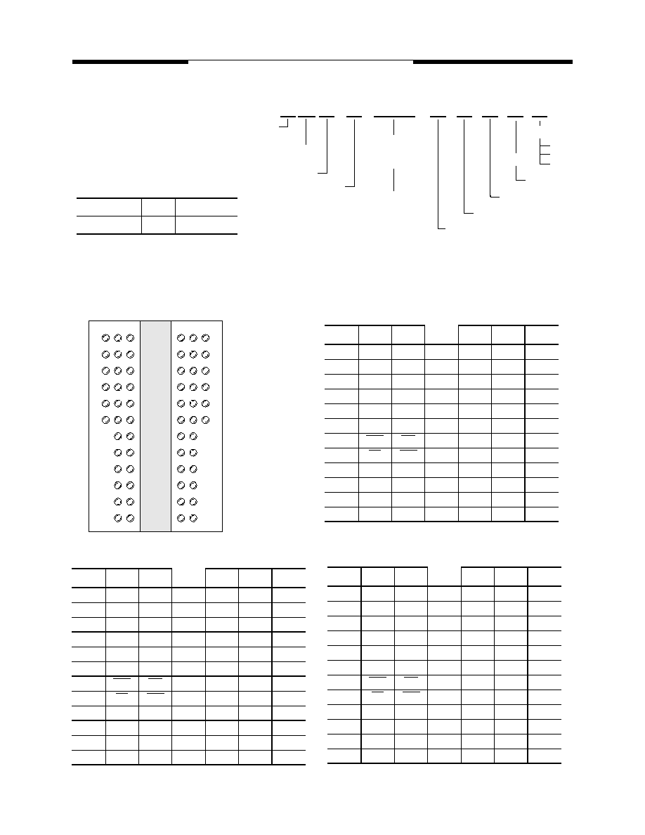
Device Usage Chart
Operating
Temperature
Range
Package Outline
Access Time (ns)
Power
Temperature
Mark
B
6
7PC
7
8PC
Std.
L
0
�
C to 70
�
C
�
�
�
�
�
�
�
Blank
MOSEL VITELIC
V54C3128(16/80/40)4V(BGA)
3
V54C3128(16/80/40)4V(BGA) Rev. 1.3 November 2002
Capacitance*
T
A
= 0 to 70
�
C, V
CC
= 3.3 V
�
0.3 V, f = 1 Mhz
*Note:Capacitance is sampled and not 100% tested.
Absolute Maximum Ratings*
Operating temperature range .................. 0 to 70 �C
Storage temperature range ................-55 to 150 �C
Input/output voltage.................. -0.3 to (V
CC
+0.3) V
Power supply voltage .......................... -0.3 to 4.6 V
Power dissipation ..............................................1 W
Data out current (short circuit).......................50 mA
*Note:
Stresses above those listed under "Absolute Maximum
Ratings" may cause permanent damage of the device.
Exposure to absolute maximum rating conditions for
extended periods may affect device reliability.
Symbol
Parameter
Max. Unit
C
I1
Input Capacitance (A0 to A11)
3.8
pF
C
I2
Input Capacitance
RAS, CAS, WE, CS, CLK, CKE, DQM
3.8
pF
C
IO
Output Capacitance (I/O)
6
pF
C
CLK
Input Capacitance (CLK)
3.5
pF
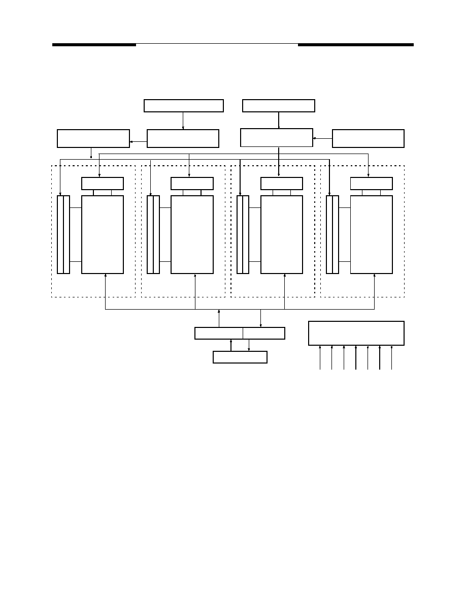
Block Diagram
Row decoder
Memory array
Bank 0
4096 x 512
x 16 bit
C
o
l
u
mn
dec
oder
S
ens
e
ampl
i
f
i
e
r
&
I(
O
)
bus
Row decoder
Memory array
Bank 1
4096 x 512
x16 bit
C
o
l
u
mn d
e
c
o
der
S
e
ns
e
ampl
i
f
i
e
r
&
I(
O
)
bus
Row decoder
Memory array
Bank 2
4096 x 512
x 16 bit
Co
l
u
m
n
d
e
c
o
d
e
r
S
ens
e
ampl
i
f
i
e
r
&
I(
O
)
bus
Row decoder
Memory array
Bank 3
4096 x 512
x 16 bit
Co
l
u
m
n
d
e
c
o
d
e
r
S
ens
e ampl
i
f
i
e
r
&
I
(
O
)
bus
Input buffer
Output buffer
I/O
1
-I/O
16
Column address
counter
Column address
buffer
Row address
buffer
Refresh Counter
A0 - A11, BA0, BA1
A0 - A8, AP, BA0, BA1
Control logic & timing generator
CL
K
CK
E
CS
RA
S
CA
S
WE
LD
Q
M
Row Addresses
Column Addresses
UDQM
x16 Configuration
5
V54C3128(16/80/40)4V(BGA) Rev. 1.3 November 2002
MOSEL VITELIC
V54C3128(16/80/40)4V(BGA)
Block Diagram
x4 Configuration
Row decoder
Memory array
Bank 0
4096 x 2048
x 4 bit
Co
l
u
m
n
d
e
c
o
d
e
r
S
ens
e am
pl
i
f
i
e
r
&
I(
O
)
bus
Row decoder
Memory array
Bank 1
4096 x 2048
x 4 bit
C
o
l
u
m
n
dec
oder
S
ens
e am
pl
i
f
i
e
r
&
I(
O
)
bus
Row decoder
Memory array
Bank 2
4096 x 2048
x 4 bit
C
o
l
u
mn
dec
oder
S
ens
e am
pl
i
f
i
e
r
&
I(
O
)
bus
Row decoder
Memory array
Bank 3
4096 x 2048
x 4 bit
C
o
l
u
mn
dec
oder
S
ens
e a
m
pl
i
f
i
e
r
&
I(
O
)
bu
s
Input buffer
Output buffer
I/O
1
-I/O
4
Column address
counter
Column address
buffer
Row address
buffer
Refresh Counter
A0 - A11, BA0, BA1
A0 - A9, A11, AP, BA0, BA1
Control logic & timing generator
CL
K
CK
E
CS
RA
S
CA
S
WE
DQM
Row Addresses
Column Addresses