MOSEL VITELIC
1
V54C316162V
200/183/166/143 MHz 3.3 VOLT, 4K REFRESH
ULTRA HIGH PERFORMANCE
1M X 16 SDRAM 2 BANKS X 512Kbit X 16
V54C316162V Rev.2.9 September 2001
V54C316162V
-5
-55
-6
-7
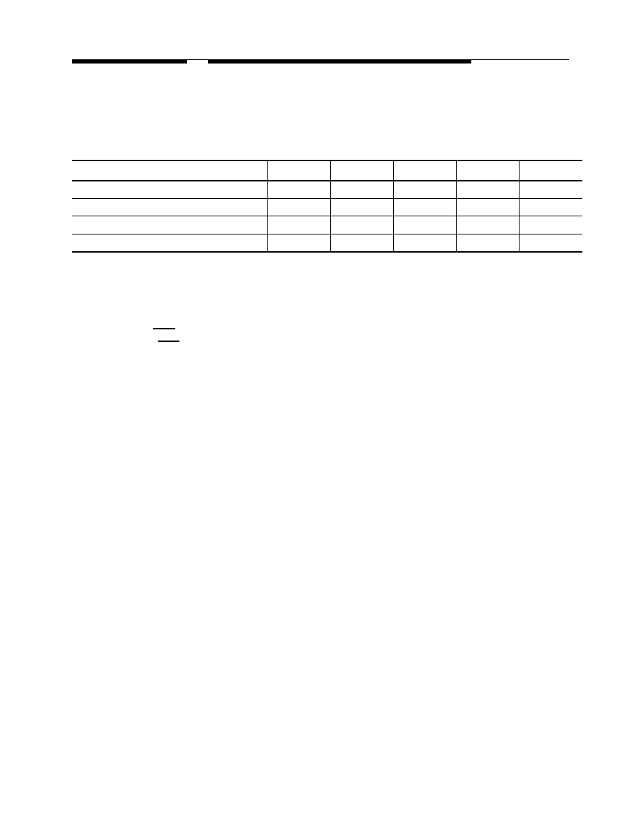
Unit
Clock Frequency (t
CK
)
200
183
166
143
MHz
Latency
3
3
3
3
clocks
Cycle Time (t
CK
)
5
5.5
6
7
ns
Access Time (t
AC
)
5
5.3
5.5
5.5
ns
Features
s
JEDEC Standard 3.3V Power Supply
s
The V54C316162V is ideally suited for high per-
formance graphics peripheral applications
s
Single Pulsed RAS Interface
s
Programmable CAS Latency: 2, 3
s
All Inputs are sampled at the positive going edge
of clock
s
Programmable Wrap Sequence: Sequential or
Interleave
s
Programmable Burst Length: 1, 2, 4, 8 and Full
Page for Sequential and 1, 2, 4, 8 for Interleave
s
UDQM & LDQM for byte masking
s
Auto & Self Refresh
s
4K Refresh Cycles/64 ms
s
Burst Read with Single Write Operation
Description
The V54C316162V is a 16,777,216 bits synchro-
nous high data rate DRAM organized as 2 x
524,288 words by 16 bits. The device is designed to
comply with JEDEC standards set for synchronous
DRAM products, both electrically and mechanically.
Synchronous design allows precise cycle control
with the system clock. The CAS latency, burst
length and burst sequence must be programmed
into device prior to access operation.

2
V54C316162V Rev. 2.9 September 2001
MOSEL VITELIC
V54C316162V
50 Pin Plastic TSOP-II
PIN CONFIGURATION
Top View
Pin Names
V
CC
I/O
1
I/O
2
V
SSQ
I/O
3
I/O
4
V
CCQ
I/O
5
I/O
6
V
SSQ
I/O
7
I/O
8
V
CCQ
LDQM
WE
CAS
RAS
CS
BA
A
10
A
0
A
1
A
2
A
3
V
CC
V
SS
I/O
16
I/O
15
V
SSQ
I/O
14
I/O
13
V
CCQ
I/O
12
I/O
11
V
SSQ
I/O
10
I/O
9
V
CCQ
NC
UDQM
CLK
CKE
NC
A
9
A
8
A
7
A
6
A
5
A
4
V
SS
1
2
3
4
5
6
7
8
9
10
11
12
13
14
15
16
17
18
19
20
21
22
23
24
25
50
49
48
47
46
45
44
43
42
41
40
39
38
37
36
35
34
33
32
31
30
29
28
27
26
V54C316162V-01
CLK
Clock Input
CKE
Clock Enable
CS
Chip Select
RAS
Row Address Strobe
CAS
Column Address Strobe
WE
Write Enable
A
0
≠A
10
Address Inputs
BA
Bank Select
I/O
1
≠I/O
16
Data Input/Output
LDQM, UDQM
Data Mask
V
CC
Power (+3.3V)
V
SS
Ground
V
CCQ
Power for I/O's (+3.3V)
V
SSQ
Ground for I/O's
NC
Not connected
4
V54C316162V Rev.2.9 September 2001
MOSEL VITELIC
V54C316162V
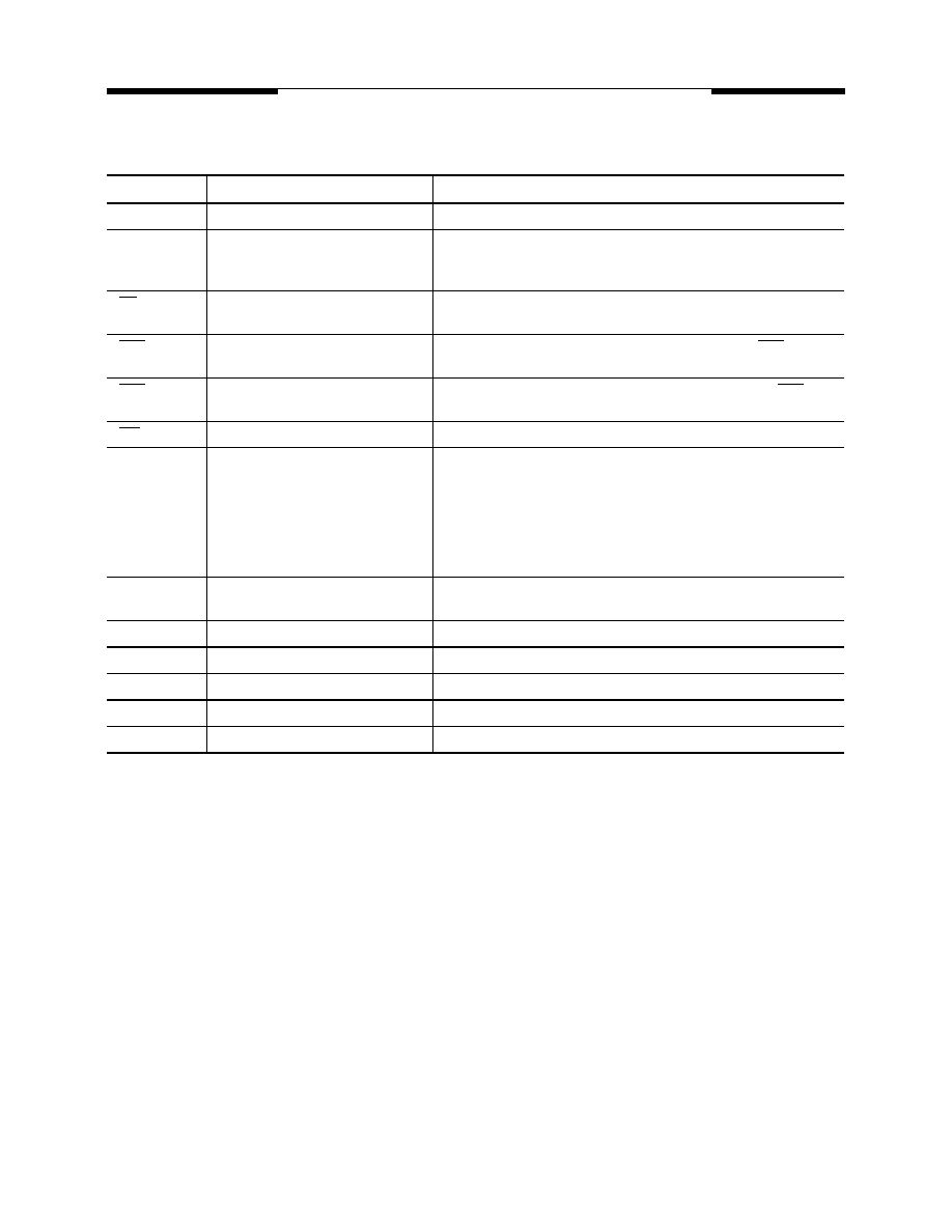
Signal Pin Description
Pin
Name
Input Function
CLK
Clock Input
System clock input. Active on the positive rising edge to sample all inptus
CKE
Clock Enable
Activates the CLK signal when high and deactivates the CLK when low.
CKE low initiates the power down mode, suspend mode, or the self
refresh mode
CS
Chip Select
Disables or enables device operation by masking or enabling all inputs
except CLK, CKE and DQMi
RAS
Row Address Strobe
Latches row addresses on the positive edge of CLK with RAS low.
Enables row access & precharge
CAS
Column Address Strobe
Latches column addresses on the positive edge of CLK with CAS low.
Enables column access
WE
Write Enable
Enables write operation
A
0
-A
10
Address
During a bank activate command, A
0
-A
10
defines the row address.
During a read or write command, A
0
-A
7
defines the column address. In
addition to the column address A
10
is used to invoke auto precharge BA
define the bank to be precharged. A
10
is low, auto precharge is disabled
during a precharge cycle, If A
10
is high, both bank will be precharged ,
if A
10
is low, the BA is used to decide which bank to precharge. If A
10
is
high, all banks will be precharged.
BA
Bank Select
Selects which bank to activate. BA low select bank A and high selects
bank B
I/O
1
-I/O
16
Data Input/Output
Data inputs/output are multiplexed on the same pins
UDQM, LDQM
Data Input/Output Mask
Makes data output Hi-Z. Blocks data input when DQM is active
VDD/VSS
Power Supply/Ground
Power Supply. +3.3V ± 0.3V/ground
VDDQ/VSSQ
Data Output Power/Ground
Provides isolated power/ground to DQs for improved noise immunity
NC
No Connection
5
V54C316162V Rev. 2.9 September 2001
MOSEL VITELIC
V54C316162V
Address Input for Mode Set (Mode Register Operation)
Power On and Initialization
The default power on state of the mode register is
supplier specific and may be undefined. The
following power on and initialization sequence
guarantees the device is preconditioned to each
users specific needs. Like a conventional DRAM,
the Synchronous DRAM must be powered up and
initialized in a predefined manner. During power on,
all VCC and VCCQ pins must be built up
simultaneously to the specified voltage when the
input signals are held in the "NOP" state. The power
on voltage must not exceed VCC+0.3V on any of
the input pins or VCC supplies. The CLK signal
must be started at the same time. After power on,
an initial pause of 200
µ
s is required followed by a
precharge of both banks using the precharge
command. To prevent data contention on the DQ
bus during power on, it is required that the DQM and
CKE pins be held high during the initial pause
period. Once all banks have been precharged, the
Mode Register Set Command must be issued to
initialize the Mode Register. A minimum of eight
Auto Refresh cycles (CBR) are also required.These
may be done before or after programming the Mode
Register. Failure to follow these steps may lead to
unpredictable start-up modes.
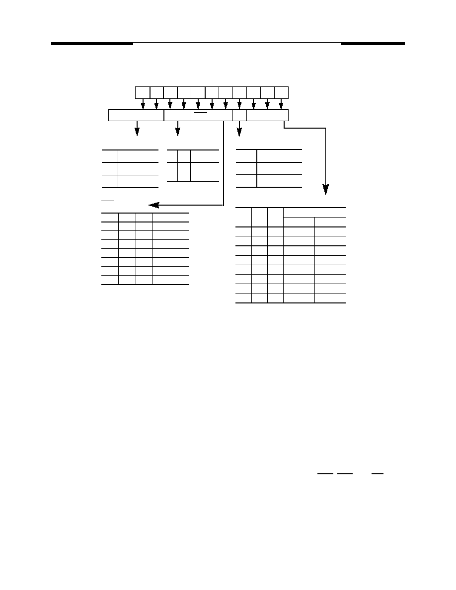
Programming the Mode Register
The Mode register designates the operation
mode at the read or write cycle. This register is di-
vided into 4 fields. A Burst Length Field to set the
length of the burst, an Addressing Selection bit to
program the column access sequence in a burst
cycle (interleaved or sequential), a CAS Latency
Field to set the access time at clock cycle and a Op-
eration mode field to differentiate between normal
operation (Burst read and burst Write) and a special
Burst Read and Single Write mode. The mode set
operation must be done before any activate com-
mand after the initial power up. Any content of the
mode register can be altered by re-executing the
mode set command. All banks must be in pre-
charged state and CKE must be high at least one
clock before the mode set operation. After the mode
register is set, a Standby or NOP command is
required. Low signals of RAS, CAS, and WE at the
positive edge of the clock activate the mode set
operation. Address input data at this timing defines
parameters to be set as shown in the previous table.
A3
A4
A2
A1
A0
A9
A8
A7
A6
A5
Address Bus (Ax)
BT
Burst Length
CAS Latency
Mode Register
CAS Latency
A6
A5
A4
Latency
0
0
0
Reserve
0
0
1
Reserve
0
1
0
2
0
1
1
3
1
0
1
Reserve
1
1
0
Reserve
1
1
1
Reserve
Burst Length
A2
A1
A0
Length
Sequential
Interleave
0
0
0
1
1
0
0
1
2
2
0
1
0
4
4
0
1
1
8
8
1
0
0
Reserve
Reserve
1
0
1
Reserve
Reserve
1
1
0
Reserve
Reserve
1
1
1
Full Page
Reserve
Burst Type
A3
Type
0
Sequential
1
Interleave
Test Mode
A8
A7
Mode
0
0
Mode Reg
Set
Test
Mode
Write Burst Length
Write Burst Length
A9
Length
0
Burst
1
Single Bit
A10
