
MOSEL VITELIC
1
V54C31732G2V
HIGH PERFORMANCE 166/143 MHz
3.3 VOLT ENHANCED GRAPHICS
512K X 32 SDRAM 2 BANKS X 256Kbit X 32
V54C31732G2V Rev. 1.0 August 1999
PRELIMINARY
V54C31732G2V
-6
-7
-8
-10
Unit
Clock Frequency (t
CK
)
166
143
125
100
MHz
Latency
3
3
3
3
clocks
Cycle Time (t
CK
)
6
7
8
10
ns
Access Time (t
AC
)
5.4
5.4
6
7
ns
Features
s
JEDEC Standard 3.3V Power Supply
s
Specially screened for graphics applications
s
Single Pulsed RAS Interface
s
Programmable CAS Latency: 2, 3
s
All Inputs are sampled at the positive going edge
of clock
s
Programmable Wrap Sequence: Sequential or
Interleave
s
Programmable Burst Length: 1, 2, 4, 8 and Full
Page for Sequential and 1, 2, 4, 8 for Interleave
s
DQM 0-3 for Byte Masking
s
Auto & Self Refresh
s
2K Refresh Cycles/32 ms
s
Special Mode Registers
s
One Color Register
s
Burst Read with Single Write Operation
s
Block Write (8 Columns)
Description
The V54C31732G2V is a 33,554,432 bits syn-
chronous high data rate DRAM organized as 2 x
262,144 words by 32 bits. The device is designed to
comply with JEDEC standards set for synchronous
DRAM products, both electrically and mechanically.
Synchronous design allows precise cycle control
with the system clock. The CAS latency, burst
length and burst sequence must be programmed
into device prior to access operation. In addition, it
features block write and masked block write func-
tions by making a programmable mode register and
special mode register, the system can select modes
to maximize its performance.
2
V54C31732G2V Rev. 1.0 August 1999
MOSEL VITELIC
V54C31732G2V
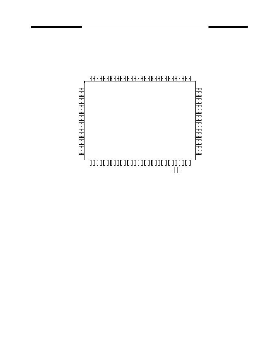
100 Pin TQFP
PIN CONFIGURATION
Top View
81
82
83
84
85
86
87
88
89
90
91
92
93
94
95
96
97
98
99
100
50
49
48
47
46
45
44
43
42
41
40
39
38
37
36
35
34
33
32
31
80
79
78
77
76
75
74
73
72
71
70
69
68
67
66
65
64
63
62
61
60
59
58
57
56
55
54
53
52
51
1
2
3
4
5
6
7
8
9
10
11
12
13
14
15
16
17
18
19
20
21
22
23
24
25
26
27
28
29
30
DQ
29
VSSQ
DQ
30
DQ
31
V
SS
NC
NC
NC
NC
NC
NC
NC
NC
NC
NC
VDD
DQ
0
DQ
1
VSSQ
DQ
2
A
7
A
6
A
5
A
4
V
SS
NC
NC
NC
NC
NC
NC
NC
NC
NC
NC
VDD
A
3
A
2
A
1
A
0
DQ
3
VDDQ
DQ
4
DQ
5
VSSQ
DQ
6
DQ
7
VDDQ
DQ
16
DQ
17
VSSQ
DQ
18
DQ
19
VDDQ
VDD
V
SS
DQ
20
DQ
21
VSSQ
DQ
22
DQ
23
VDDQ
DQM
0
DQM
2
WE
CAS
RAS
CS
BA
A
8
DQ
28
VDDQ
DQ
27
DQ
26
VSSQ
DQ
25
DQ
24
VDDQ
DQ
15
DQ
14
VSSQ
DQ
13
DQ
12
VDDQ
V
SS
VDD
DQ
11
DQ
10
VSSQ
DQ
9
DQ
8
VDDQ
NC
DQM
3
DQM1
CLK
CKE
DSF
NC
A
9
/A
P
100 pin TQFP
20 x 14 mm
2
0.65 mm pitch
(Marking side)
V54C31732G2V-01
MOSEL VITELIC
V54C31732G2V
3
V54C31732G2V Rev. 1.0 August 1999
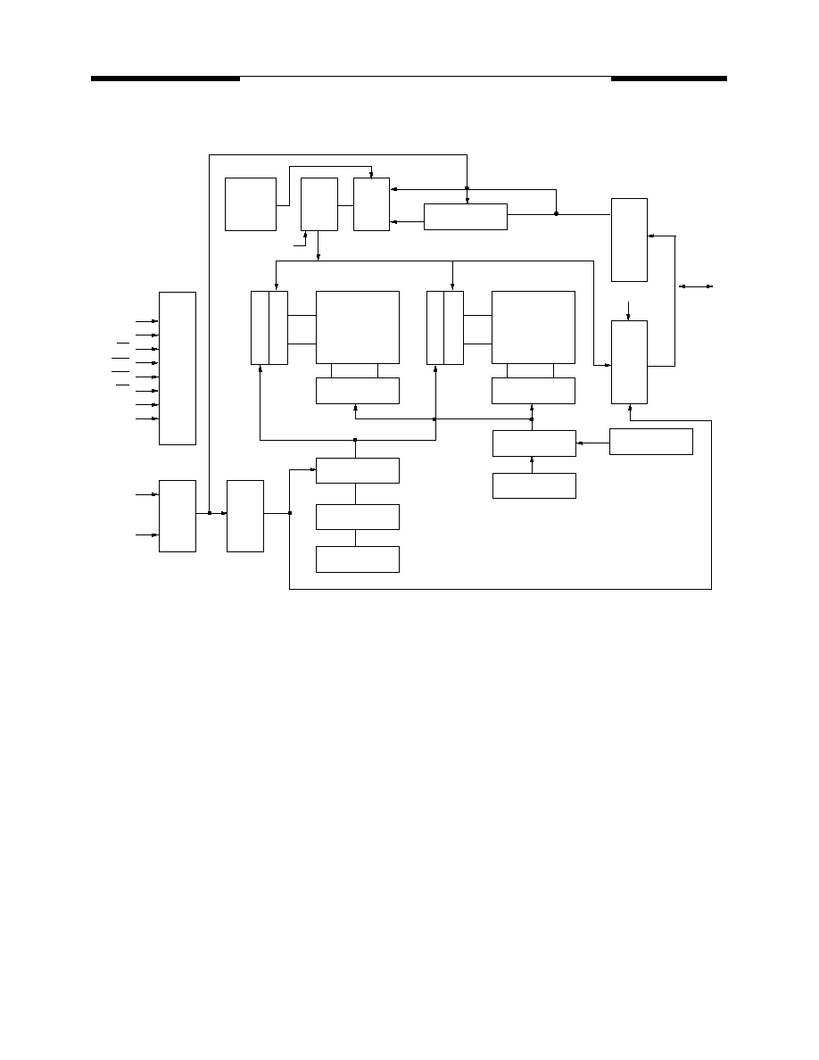
Block Diagram
V54C31732G2V-02
CLK
CKE
CS
RAS
CAS
WE
DSF
DQMi
CLK
Address
A
0
-A
7
, BA
Column Address
Buffer
Row Address
Buffer
Refresh
Counter
Latency 8
Burst Length
Output
Buff
er
Input
Buff
er
Prog
r
amming
Register
Column Decoder
Sense Amplifier
Timing
Register
Column Address
Counter
Row
Decoder
MUX
Write
Control
Logic
Block
Write
Control
Logic
Memory Array
Bank 0
256k x 32
Memory Array
Bank 1
256k x 32
Row
Decoder
Color
Register
DQMi
DQMi
DQ
0
-DQ
31
Column Addresses
A
0
-A
9
, BA
Row Addresses
Column Decoder
Sense Amplifier
4
V54C31732G2V Rev. 1.0 August 1999
MOSEL VITELIC
V54C31732G2V
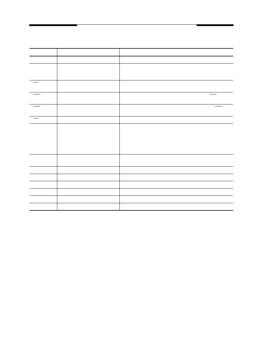
Signal Pin Description
Pin
Name
Input Function
CLK
Clock Input
System clock input. Active on the positive rising edge to sample all inptus
CKE
Clock Enable
Activates the CLK signal when high and deactivates the CLK when low.
CKE low initiates the power down mode, suspend mode, or the self
refresh mode
CS
Chip Select
Disables or enables device operation by masking or enabling all inputs
except CLK, CKE and DQMi
RAS
Row Address Strobe
Latches row addresses on the positive edge of CLK with RAS low.
Enables row access & precharge
CAS
Column Address Strobe
Latches column addresses on the positive edge of CLK with CAS low.
Enables column access
WE
Write Enable
Enables write operation
A
0
-A
9
Address
During a bank activate command, A
0
-A
9
defines the row address. During
a read or write command, A
0
-A
7
defines the column address. In addition
to the column address A
9
is used to invoke auto precharge BA define the
bank to be precharged. A
9
is low, auto precharge is disabled during a
precharge cycle, If A
9
is high, both bank will be precharged ,if A
9
is low,
the BA is used to decide which bank to precharge
BA
Bank Select
Selects which bank to activate. BA low select bank A and high selects
bank B
DQ
0
-DQ
31
Data Input/Output
Data inputs/output are multiplexed on the same pins
DQMi
Data Input/Output Mask
Makes data output Hi-Z. Blocks data input when DQM is active
VDD/VSS
Power Supply/Ground
Power Supply. +3.3V
�
0.3V/ground
VDDQ/VSSQ
Data Output Power/Ground
Provides isolated power/ground to DQs for improved noise immunity
DSF
Define Special Function
Enables block write and special mode register set
NC
No Connection
5
V54C31732G2V Rev. 1.0 August 1999
MOSEL VITELIC
V54C31732G2V
Address Input for Mode Set (Mode Register Operation)
Power On and Initialization
The default power on state of the mode register is
supplier specific and may be undefined. The
following power on and initialization sequence
guarantees the device is preconditioned to each
users specific needs. Like a conventional DRAM,
the Synchronous DRAM must be powered up and
initialized in a predefined manner. During power on,
all VCC and VCCQ pins must be built up
simultaneously to the specified voltage when the
input signals are held in the "NOP" state. The power
on voltage must not exceed VCC+0.3V on any of
the input pins or VCC supplies. The CLK signal
must be started at the same time. After power on,
an initial pause of 200
�
s is required followed by a
precharge of both banks using the precharge
command. To prevent data contention on the DQ
bus during power on, it is required that the DQM and
CKE pins be held high during the initial pause
period. Once all banks have been precharged, the
Mode Register Set Command must be issued to
initialize the Mode Register. A minimum of eight
Auto Refresh cycles (CBR) are also required.These
may be done before or after programming the Mode
Register. Failure to follow these steps may lead to
unpredictable start-up modes.
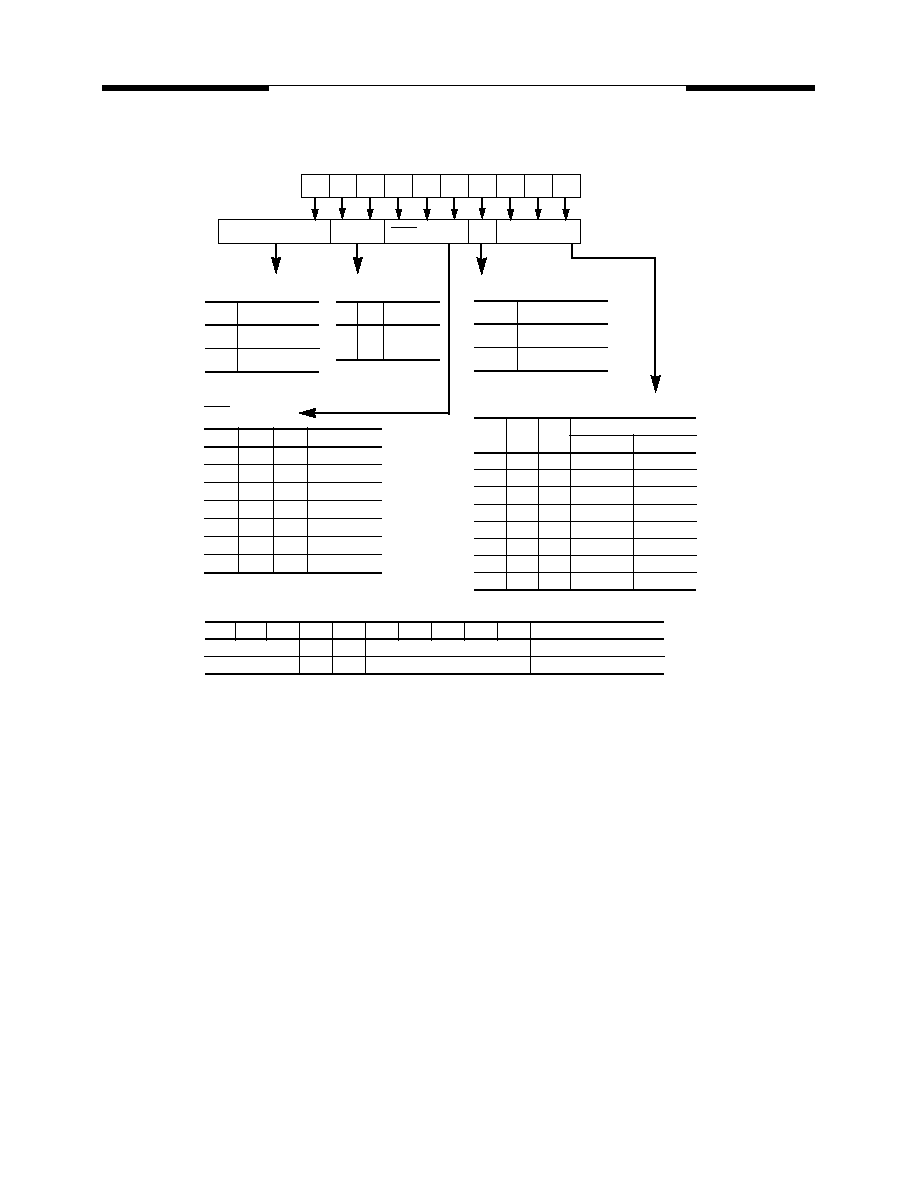
Programming the Mode Register
The Mode register designates the operation
mode at the read or write cycle. This register is di-
vided into 4 fields. A Burst Length Field to set the
length of the burst, an Addressing Selection bit to
program the column access sequence in a burst cy-
cle (interleaved or sequential), a CAS
Latency
Field
to set the access time at clock cycle and a Opera-
tion mode field to differentiate between normal op-
eration (Burst read and burst Write) and a special
Burst Read and Single Write mode. The mode set
operation must be done before any activate com-
mand after the initial power up. Any content of the
A3
A4
A2
A1
A0
A9
A8
A7
A6
A5
Address Bus (Ax)
BT
Burst Length
CAS Latency
Mode Register
CAS Latency
A6
A5
A4
Latency
0
0
0
Reserve
0
0
1
Reserve
0
1
0
2
0
1
1
3
1
0
1
Reserve
1
1
0
Reserve
1
1
1
Reserve
Burst Length
A2
A1
A0
Length
Sequential
Interleave
0
0
0
1
1
0
0
1
2
2
0
1
0
4
4
0
1
1
8
8
1
0
0
Reserve
Reserve
1
0
1
Reserve
Reserve
1
1
0
Reserve
Reserve
1
1
1
Full Page
Reserve
Burst
Type
A3
Type
0
Sequential
1
Interleave
Test Mode
A8
A7
Mode
0
0
Mode Reg
Set
Test
Mode
Write Burst Length
Write Burst Length
A9
Length
0
Burst
1
Single Bit
Special Mode Set SMRS
A9
A8
A7
A6
A5
A4
A3
A2
A1
A0
Functions
X
0
X
X
Unchanged
X
1
X
X
Load Color Register