V55C2128164V(T_B)(1.2).fm
MOSEL VITELIC
1
V55C2128164V(T/B)
128Mbit LOW-POWER SDRAM
2.5 VOLT, TSOP II / BGA PACKAGE
8M X 16
V55C2128164V(T/B) Rev. 1.2 August 2002
PRELIMINARY
6
7PC
7
8PC
10
System Frequency (f
CK
)
166 MHz
143 MHz
143 MHz
125 MHz
100MHz
Clock Cycle Time (t
CK3
)
6 ns
7 ns
7 ns
8 ns
10 ns
Clock Access Time (t
AC3
) CAS Latency = 3
5.4 ns
5.4 ns
5.4 ns
6 ns
7 ns
Clock Access Time (t
AC2
) CAS Latency = 2
5.4 ns
5.4 ns
6 ns
6 ns
8 ns
Clock Access Time (t
AC1
) CAS Latency = 1
19 ns
19 ns
19 ns
19 ns
22 ns
Features
4 banks x 2Mbit x 16 organization
High speed data transfer rates up to 166 MHz
Full Synchronous Dynamic RAM, with all signals
referenced to clock rising edge
Single Pulsed RAS Interface
Data Mask for Read/Write Control
Four Banks controlled by BA0 & BA1
Programmable CAS Latency:1, 2, 3
Programmable Wrap Sequence: Sequential or
Interleave
Programmable Burst Length:
1, 2, 4, 8, Full page for Sequential Type
1, 2, 4, 8 for Interleave Type
Multiple Burst Read with Single Write Operation
Automatic and Controlled Precharge Command
Random Column Address every CLK (1-N Rule)
Power Down Mode and Clock Suspend Mode
Deep Power Mode
Auto Refresh and Self Refresh
Refresh Interval: 4096 cycles/64 ms
Available in 54-ball FBGA, with 9x6 ball array
with 3 depupulated rows, 9x8 mm and 54 pin
TSOP II
VDD=2.5V, VDDQ=1.8V
Programmable Power Reduction Feature by par-
tial array activation during Self-Refresh
Operating Temperature Range
Commercial (
0
�
C to 70
�
C)
Extended (-25
�
C to +85
�
C)
Device Usage Chart
Operating
Temperature
Range
Package Outline
Access Time (ns)
Temperature
Mark
T/B
6
7PC
7
8PC
10
0
�
C to 70
�
C
�
�
�
�
�
�
Commercial
-25
�
C to 85
�
C
�
�
�
�
�
�
Extended
2
V55C2128164V(T/B) Rev.1.2 August 2002
MOSEL VITELIC
V55C2128164V(T/B)
60 Pin WBGA PIN CONFIGURATION
Top View
Description
Pkg.
Pin Count
BGA
B
54
V 55 C 2 12816 4 S X B
Mosel Vitelic
Manufactured
Low Power
Synchronous DRAM
C=CMOS Family
2.5V Supply Voltage
128Mb(4K Refresh)
4 Banks
S=SSTL
Component Rev Level
Component
Package
Device
Number
Speed
6 ns
7 ns
8 ns
A = 0.14um
10 ns
Pin Configuration for x16 devices:
< Top-view >
1
2
3
7
8
9
VSS DQ15 VSSQ
A
VDDQ DQ0
VDD
DQ14 DQ13 VDDQ
B
VSSQ DQ2
DQ1
DQ12 DQ11 VSSQ
C
VDDQ DQ4
DQ3
DQ10 DQ9 VDDQ
D
VSSQ DQ6
DQ5
DQ8
NC
VSS
E
VDD LDQM DQ7
UDQM CLK
CKE
F
CAS
RAS
WE
NC
A11
A9
G
BA0
BA1
CS
A8
A7
A6
H
A0
A1
A10
VSS
A5
A4
J
A3
A2
VDD
3
V55C2128164V(T/B) Rev. 1.2 August 2002
MOSEL VITELIC
V55C2128164V(T/B)
54 Pin Plastic TSOP-II
PIN CONFIGURATION
Top View
Pin Names
V
CC
I/O
1
V
CCQ
I/O
2
I/O
3
V
SSQ
I/O
4
I/O
5
V
CCQ
I/O
6
I/O
7
V
SSQ
I/O
8
V
CC
LDQM
WE
CAS
RAS
CS
BA0
BA1
A
10
A
0
A
1
A
2
A
3
V
CC
V
SS
I/O
16
V
SSQ
I/O
15
I/O
14
V
CCQ
I/O
13
I/O
12
V
SSQ
I/O
11
I/O
10
V
CCQ
I/O
9
V
SS
NC
UDQM
CLK
CKE
NC
A
11
A
9
A
8
A
7
A
6
A
5
A
4
V
SS
1
2
3
4
5
6
7
8
9
10
11
12
13
14
15
16
17
18
19
20
21
22
23
24
25
26
27
54
53
52
51
50
49
48
47
46
45
44
43
42
41
40
39
38
37
36
35
34
33
32
31
30
29
28
CLK
Clock Input
CKE
Clock Enable
CS
Chip Select
RAS
Row Address Strobe
CAS
Column Address Strobe
WE
Write Enable
A
0
�A
11
Address Inputs
BA0, BA1
Bank Select
I/O
1
�I/O
16
Data Input/Output
LDQM, UDQM
Data Mask
V
CC
Power (+2.5V)
V
SS
Ground
V
CCQ
Power for I/O's (+1.8V)
V
SSQ
Ground for I/O's
NC
Not connected
V 55 C 2 12816 4 S X T
Mosel Vitelic
Manufactured
Low Power
Synchronous DRAM
C=CMOS Family
2.5V Supply Voltage
8Mx16(4K Refresh)
4 Banks
S=STTL
Component Rev Level
Component
Package
Speed
6 ns
7 ns
8 ns
Device
Number
A = 0.14um
10 ns
Description
Pkg.
Pin Count
TSOP-II
T
54
4
V55C2128164V(T/B) Rev. 1.2 August 2002
MOSEL VITELIC
V55C2128164V(T/B)
Description
The V55C2128164V(T/B) is a four bank Synchronous DRAM organized as 4 banks x 2Mbit x 16. The
V55C2128164V(T/B) achieves high speed data transfer rates up to 166 MHz by employing a chip architecture
that prefetches multiple bits and then synchronizes the output data to a system clock
All of the control, address, data input and output circuits are synchronized with the positive edge of an ex-
ternally supplied clock.
Operating the four memory banks in an interleaved fashion allows random access operation to occur at
higher rate than is possible with standard DRAMs. A sequential and gapless data rate of up to 166 MHz is
possible depending on burst length, CAS latency and speed grade of the device.
Signal Pin Description
Pin
Type
Signal
Polarity
Function
CLK
Input
Pulse
Positive
Edge
The system clock input. All of the SDRAM inputs are sampled on the rising edge of the
clock.
CKE
Input
Level
Active High Activates the CLK signal when high and deactivates the CLK signal when low, thereby
initiates either the Power Down mode or the Self Refresh mode.
CS
Input
Pulse
Active Low CS enables the command decoder when low and disables the command decoder when
high. When the command decoder is disabled, new commands are ignored but previous
operations continue.
RAS, CAS
WE
Input
Pulse
Active Low When sampled at the positive rising edge of the clock, CAS, RAS, and WE define the
command to be executed by the SDRAM.
A0 - A11
Input
Level
--
During a Bank Activate command cycle, A0-A11 defines the row address (RA0-RA11)
when sampled at the rising clock edge.
During a Read or Write command cycle, A0-An defines the column address (CA0-CAn)
when sampled at the rising clock edge.CAn depends from the SDRAM organization:
� 8M x 16 SDRAM CA0�CA8.
In addition to the column address, A10(=AP) is used to invoke autoprecharge operation
at the end of the burst read or write cycle. If A10 is high, autoprecharge is selected and
BA0, BA1 defines the bank to be precharged. If A10 is low, autoprecharge is disabled.
During a Precharge command cycle, A10(=AP) is used in conjunction with BA0 and BA1
to control which bank(s) to precharge. If A10 is high, all four banks will BA0 and BA1 are
used to define which bank to precharge.
BA0,
BA1
Input
Level
--
Selects which bank is to be active.
DQx
Input
Output
Level
--
Data Input/Output pins operate in the same manner as on conventional DRAMs.
LDQM
UDQM
Input
Pulse
Active High The Data Input/Output mask places the DQ buffers in a high impedance state when sam-
pled high. In Read mode, DQM has a latency of two clock cycles and controls the output
buffers like an output enable. In Write mode, DQM has a latency of zero and operates as
a word mask by allowing input data to be written if it is low but blocks the write operation
if DQM is high.
VCC, VSS
Supply
Power and ground for the input buffers and the core logic.
VCCQ
VSSQ
Supply
--
--
Isolated power supply and ground for the output buffers to provide improved noise
immunity.
5
V55C2128164V(T/B) Rev. 1.2 August 2002
MOSEL VITELIC
V55C2128164V(T/B)
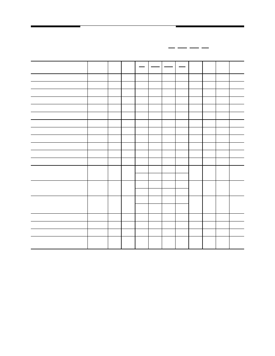
Operation Definition
All of SDRAM operations are defined by states of control signals CS, RAS, CAS, WE, and DQM at the
positive edge of the clock. The following list shows the thruth table for the operation commands.
Notes:
1.
V = Valid , x = Don't Care, L = Low Level, H = High Level
2.
CKEn signal is input level when commands are provided, CKEn-1 signal is input level one clock before the commands
are provided.
3.
These are state of bank designated by BS0, BS1 signals.
4.
Power Down Mode can not entry in the burst cycle.
5. After Deep Power Down mode exit a full new initialization of memory device is mandatory
Operation
Device
State
CKE
n-1
CKE
n
CS
RAS
CAS
WE
DQM
A0-9,
A11
A10
BS0
BS1
Row Activate
Idle
3
H
X
L
L
H
H
X
V
V
V
Read
Active
3
H
X
L
H
L
H
X
V
L
V
Read w/Autoprecharge
Active
3
H
X
L
H
L
H
X
V
H
V
Write Active
3
H
X
L
H
L
L
X
V
L
V
Write with Autoprecharge
Active
3
H
X
L
H
L
L
X
V
H
V
Row Precharge
Any
H
X
L
L
H
L
X
X
L
V
Precharge All
Any
H
X
L
L
H
L
X
X
H
X
Mode Register Set
Idle
H
X
L
L
L
L
X
V
V
V
No Operation
Any
H
X
L
H
H
H
X
X
X
X
Device Deselect
Any
H
X
H
X
X
X
X
X
X
X
Auto Refresh
Idle
H
H
L
L
L
H
X
X
X
X
Self Refresh Entry
Idle
H
L
L
L
L
H
X
X
X
X
Self Refresh Exit
Idle
(Self Refr.)
L
H
H
X
X
X
X
X
X
X
L
H
H
X
Power Down Entry
Idle
Active
4
H
L
H
X
X
X
X
X
X
X
L
H
H
X
Power Down Exit
Any
(Power
Down)
L
H
H
X
X
X
X
X
X
X
L
H
H
L
Data Write/Output Enable
Active
H
X
X
X
X
X
L
X
X
X
Data Write/Output Disable
Active
H
X
X
X
X
X
H
X
X
X
Deep Pwoer Down Entry
Idle
H
L
L
H
H
L
H
X
X
X
Deep Pwoer Down Exit
Deep power-
Down
L
H
X
X
X
X
H
X
X
X