Äîêóìåíòàöèÿ è îïèñàíèÿ www.docs.chipfind.ru
MOSEL VITELIC
1
V58C365164S
64 Mbit DDR SDRAM
4M X 16, 3.3VOLT
V58C365164S Rev. 1.7 March 2002
PRELIMINARY
36
4
5
System Frequency (f
CK
)
275 MHz
250 MHz
200 MHz
Clock Cycle Time (t
CK3
)
3.6 ns
4 ns
5 ns
Clock Cycle Time (t
CK2.5
)
4.3ns
4.8 ns
6 ns
Clock Cycle Time (t
CK2
)
5.4ns
6 ns
7.5 ns
Features
4 banks x 1Mbit x 16 organization
High speed data transfer rates with system
frequency up to 275 MHz
Data Mask for Write Control (DM)
Four Banks controlled by BA0 & BA1
Programmable CAS Latency: 2, 2.5, 3
Programmable Wrap Sequence: Sequential
or Interleave
Programmable Burst Length:
2, 4, 8 for Sequential Type
2, 4, 8 for Interleave Type
Automatic and Controlled Precharge Command
Suspend Mode and Power Down Mode
Auto Refresh and Self Refresh
Refresh Interval: 4096 cycles/64 ms
Available in 66-pin 400 mil TSOP-II
SSTL-2 Compatible I/Os
Double Data Rate (DDR)
Bidirectional Data Strobe (DQs) for input and
output data, active on both edges
On-Chip DLL aligns DQ and DQs transitions with
CLK transitions
Differential clock inputs CLK and CLK
Power supply 3.3V ± 0.3V
VDDQ (I/O) power supply 2.5 + 0.2V
Description
The V58C365164S is a four bank DDR DRAM
organized as 4 banks x 1Mbit x 16. The
V58C365164S achieves high speed data transfer
rates by employing a chip architecture that
prefetches multiple bits and then synchronizes the
output data to a system clock
All of the control, address, circuits are synchro-
nized with the positive edge of an externally sup-
plied clock. I/O transactions are possible on both
edges of DQS.
Operating the four memory banks in an inter-
leaved fashion allows random access operation to
occur at a higher rate than is possible with standard
DRAMs. A sequential and gapless data rate is pos-
sible depending on burst length, CAS latency and
speed grade of the device.
Device Usage Chart
Operating
Temperature
Range
Package Outline
CLK Cycle Time (ns)
Power
Temperature
Mark
JEDEC 66 TSOP II
-36
-4
-5
Std.
L
0°C to 70°C
·
·
·
·
·
·
Blank
2
V58C365164S Rev. 1.7 March 2002
MOSEL VITELIC
V58C365164S
66 Pin Plastic TSOP-II
PIN CONFIGURATION
Top View
Pin Names
1
2
3
4
5
6
9
10
11
12
13
14
7
8
15
16
17
18
19
20
21
22
66
65
64
63
62
61
58
57
56
55
54
53
60
59
52
51
50
49
48
47
46
45
23
24
25
44
43
42
26
27
41
40
28
29
30
31
32
33
39
38
37
36
35
34
V
DD
DQ
0
V
DDQ
DQ
1
DQ
2
DQ
3
DQ
4
DQ
5
DQ
6
DQ
7
V
SSQ
V
DDQ
V
SSQ
NC
V
DDQ
LDQS
NC
V
DD
NC
LDM
WE
CAS
RAS
CS
NC
BA0
BA1
V
SS
DQ
15
V
SSQ
DQ
14
DQ
13
V
DDQ
V
SSQ
DQ
10
DQ
9
V
DDQ
DQ
8
NC
DQ
12
DQ
11
V
SSQ
UDQS
NC
V
REF
V
SS
UDM
CLK
CLK
CKE
NC
NC
A11
A9
A10/AP
A0
A1
A2
A3
V
DD
A8
A7
A6
A5
A4
V
SS
64M
DDR SDRAM
CLK, CLK
Differential Clock Input
CKE
Clock Enable
CS
Chip Select
RAS
Row Address Strobe
CAS
Column Address Strobe
WE
Write Enable
UDQS, LDQS
Data Strobe (Bidirectional)
A
0
A
11
Address Inputs
BA0, BA1
Bank Select
DQ
0
DQ
15
Data Input/Output
UDM, LDM
Data Mask
V
DD
Power (+3.3V)
V
SS
Ground
V
DDQ
Power for I/O's (+2.5V)
V
SSQ
Ground for I/O's
NC
Not connected
V
REF
Reference Voltage for Inputs
V 58 C 3 6516 4 S A T XX
DDRSDRAM
CMOS
3.3V VDD
4MX16, 4K Refresh
4 Banks
COMPONENT
REV LEVEL
COMPONENT
PACKAGE, T = TSOP
SSTL
SPEED
36 (275MHZ@CL3)
MOSEL VITELIC
MANUFACTURED
4 (250MHZ@CL3)
5 (200MHZ@CL3)
2.5v VDDQ
MOSEL VITELIC
V58C365164S
3
V58C365164S Rev. 1.7 March 2002
Capacitance*
T
A
= 0 to 70
°
C, V
CC
= 3.3 V
±
0.2 V, f = 1 Mhz
*Note: Capacitance is sampled and not 100% tested.
Absolute Maximum Ratings*
Operating temperature range .................. 0 to 70 °C
Storage temperature range ................-55 to 150 °C
Input/output voltage.................. -0.3 to (V
CC
+0.3) V
Power supply voltage .......................... -0.3 to 4.6 V
Power dissipation ...........................................2.0 W
Data out current (short circuit).......................50 mA
*Note: Stresses above those listed under "Absolute Maximum
Ratings" may cause permanent damage of the device.
Exposure to absolute maximum rating conditions for
extended periods may affect device reliability.
Symbol
Parameter
Max. Unit
C
I1
Input Capacitance (A0 to A11)
5
pF
C
I2
Input Capacitance
RAS, CAS, WE, CS, CKE
5
pF
C
IO
Output Capacitance (DQ)
6.5
pF
C
CLK
Input Capacitance (CCLK, CLK)
4
pF
Block Diagram
Row decoder
Memory array
Bank 0
4096 x 256
x 16 bit
C
o
l
u
mn
dec
oder
S
ens
e
ampl
i
f
i
e
r
&
I(
O
)
bus
Row decoder
Memory array
Bank 1
4096 x 256
x 16 bit
C
o
l
u
mn d
e
c
o
der
S
e
ns
e
ampl
i
f
i
e
r
&
I(
O
)
bus
Row decoder
Memory array
Bank 2
4096 x 256
x 16 bit
Co
l
u
m
n
d
e
c
o
d
e
r
S
ens
e
ampl
i
f
i
e
r
&
I(
O
)
bus
Row decoder
Memory array
Bank 3
4096 x 256
x 16 bit
Co
l
u
m
n
d
e
c
o
d
e
r
S
ens
e ampl
i
f
i
e
r
&
I
(
O
)
bus
Input buffer
Output buffer
I/Q
0
-IQ
15
Column address
counter
Column address
buffer
Row address
buffer
Refresh Counter
A0 - A11, BA0, BA1
A0 - A7, AP, BA0, BA1
Control logic & timing generator
CL
K
CK
E
CS
RA
S
CA
S
WE
UDM
Row Addresses
Column Addresses
DLL
Strobe
Gen.
Data Strobe
CLK, CLK
CL
K
LD
M
DQS
4
V58C365164S Rev. 1.7 March 2002
MOSEL VITELIC
V58C365164S
Signal Pin Description
Pin
Type
Signal
Polarity
Function
CLK
CLK
Input
Pulse
Positive
Edge
The system clock input. All inputs except DQs and DMs are sampled on the rising edge
of CLK.
CKE
Input
Level
Active High Activates the CLK signal when high and deactivates the CLK signal when low, thereby
initiates either the Power Down mode, Suspend mode, or the Self Refresh mode.
CS
Input
Pulse
Active Low CS enables the command decoder when low and disables the command decoder when
high. When the command decoder is disabled, new commands are ignored but previous
operations continue.
RAS, CAS
WE
Input
Pulse
Active Low When sampled at the positive rising edge of the clock, CAS, RAS, and WE define the
command to be executed by the SDRAM.
DQS
Input/
Output
Pulse
Active High Active on both edges for data input and output.
Center aligned to input data
Edge aligned to output data
A0 - A11
Input
Level
--
During a Bank Activate command cycle, A0-A11 defines the row address (RA0-RA11)
when sampled at the rising clock edge.
During a Read or Write command cycle, A0-An defines the column address (CA0-CAn)
when sampled at the rising clock edge.CAn depends from the SDRAM organization:
8M x 8 SDRAM CAn = CA8 (Page Length = 512 bits)
In addition to the column address, A10(=AP) is used to invoke autoprecharge operation
at the end of the burst read or write cycle. If A10 is high, autoprecharge is selected and
BA0, BA1 defines the bank to be precharged. If A10 is low, autoprecharge is disabled.
During a Precharge command cycle, A10(=AP) is used in conjunction with BA0 and BA1
to control which bank(s) to precharge. If A10 is high, all four banks will be precharged
simultaneously regardless of state of BA0 and BA1.
BA0,
BA1
Input
Level
--
Selects which bank is to be active.
DQx
Input/
Output
Level
--
Data Input/Output pins operate in the same manner as on conventional DRAMs.
DM
Input
Pulse
Active High In Write mode, DM has a latency of zero and operates as a word mask by allowing input
data to be written if it is low but blocks the write operation if is high.
VDD, VSS
Supply
Power and ground for the input buffers and the core logic.
VDDQ
VSSQ
Supply
--
--
Isolated power supply and ground for the output buffers to provide improved noise
immunity.
VREF
Input
Level
--
SSTL Reference Voltage for Inputs
5
V58C365164S Rev. 1.7 March 2002
MOSEL VITELIC
V58C365164S
Functional Description
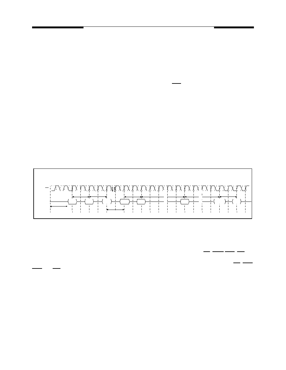
Power-Up Sequence
The following sequence is required for POWER UP.
1. Apply power and attempt to maintain CKE at a low state (all other inputs may be undefined.)
- Apply VDD before or at the same time as VDDQ.
- Apply VDDQ before or at the same time as VTT & Vref.
2. Start clock and maintain stable condition for a minimum of 200us.
3. The minimum of 200us after stable power and clock (CLK, CLK), apply NOP & take CKE high.
4. Precharge all banks.
5. Issue EMRS to enable DLL.(To issue "DLL Enable" command, provide "Low" to A0, "High" to BA0
and "Low" to all of the rest address pins, A1~A11 and BA1)
6. Issue a mode register set command for "DLL reset". The additional 200 cycles of clock input is
required to lock the DLL. (To issue DLL reset command, provide "High" to A8 and "Low" to BA0)
7. Issue precharge commands for all banks of the device.
8. Issue 2 or more auto-refresh commands.
9. Issue a mode register set command to initialize device operation.
Note1 Every "DLL enable" command resets DLL. Therefore sequence 6 can be skipped during power up. Instead of it,
the additional 200 cycles of clock input is required to lock the DLL after enabling DLL.
Extended Mode Register Set (EMRS)
The extended mode register stores the data for enabling or disabling DLL. The default value of the extend-
ed mode register is not defined, therefore the extended mode register must be written after power up for en-
abling or disabling DLL. The extended mode register is written by asserting low on CS, RAS, CAS, WE and
high on BA
0
(The DDR SDRAM should be in all bank precharge with CKE already high prior to writing into
the extended mode register). The state of address pins A
0
~ A
11
and BA
1
in the same cycle as CS, RAS,
CAS and WE low is written in the extended mode register. Two clock cycles are required to complete the
write operation in the extended mode register. The mode register contents can be changed using the same
command and clock cycle requirements during operation as long as all banks are in the idle state. A
0
is used
for DLL enable or disable. "High" on BA
0
is used for EMRS. All the other address pins except A
0
and BA
0
must be set to low for proper EMRS operation. A
1
is used at EMRS to indicate I/O strength A
1
= 0 full strength,
A
1
= 1 half strength. Refer to the table for specific codes.
Power up Sequence & Auto Refresh(CBR)
Command
0
1
2
3
4
5
6
7
8
9
10
11
12
13
14
15
16
17
18
19
t
RP
2 Clock min.
precharge
ALL Banks
2nd Auto
Refresh
Mode
Register Set
Any
Command
t
RFC
1st Auto
Refresh
t
RFC
min. 200 Cycle
· ·
CK, CK
· ·
· ·
· ·
· ·
· ·
· ·
EMRS
MRS
2 Clock min.
200
µ
S Power up
to 1st command
DLL Reset
2 Clock min.
6
5
4
7
8
8
precharge
ALL Banks
· ·