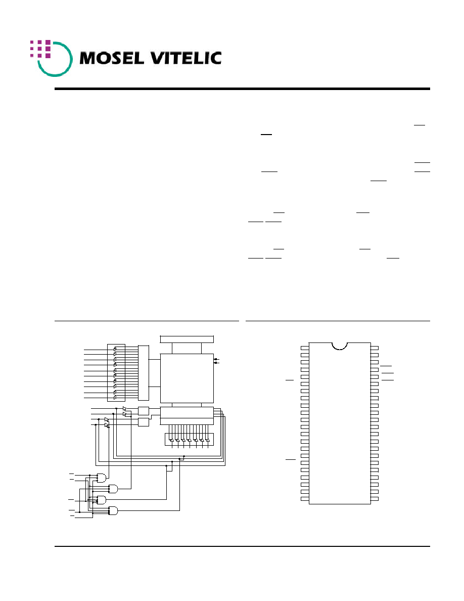
Memory Array
1024 X 2048
Row Select
I/O Circuit
Pre-Charge Circuit
Column Select
Data
Cont
Data
Cont
Vcc
Vss
A10 A11 A12 A13 A14
A9
A8
A7
A6
A5
A4
A3
A2
A1
A0
I/O1 - I/O8
I/O9 - I/O16
WE
OE
BHE
BLE
CE
A15 A16
V62C1162048L(L)
Ultra Low Power
128K x 16 CMOS SRAM
Features
� Low-power consumption
- Active: 35mA I
CC
at 70ns
- Stand-by: 10
�
A (CMOS input/output)
2
�
A (CMOS input/output, L version)
� 70/85/100/120 ns access time
� Equal access and cycle time
� Single +1.8V to2.2V Power Supply
� Tri-state output
� Automatic power-down when deselected
� Multiple center power and ground pins for
improved noise immunity
� Individual byte controls for both Read and
Write cycles
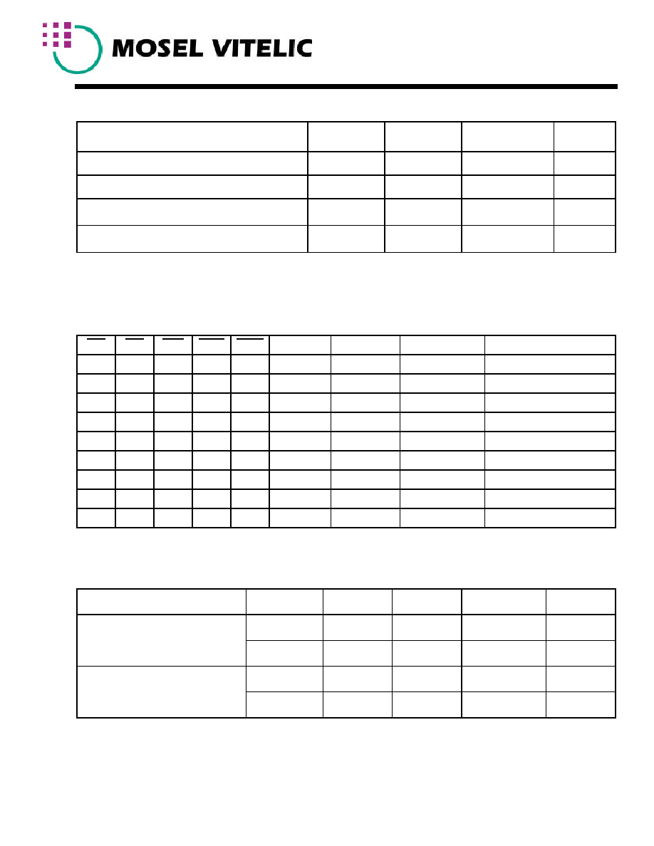
� Available in 44 pin TSOPII / 48-fpBGA / 48-
�
BGA
Functional Description
The V62C1162048L is a Low Power CMOS Static
RAM organized as 131,072 words by 16 bits. Easy
Memory expansion is provided by an active LOW (CE)
and (OE) pin.
This device has an automatic power-down mode feature
when deselected. Separate Byte Enable controls (BLE
and BHE) allow individual bytes to be accessed. BLE
controls the lower bits I/O1 - I/O8. BHE controls the
upper bits I/O9 - I/O16.
Writing to these devices is performed by taking Chip
Enable (CE) with Write Enable (WE) and Byte Enable
(BLE/BHE) LOW.
Reading from the device is performed by taking Chip
Enable (CE) with Output Enable (OE) and Byte Enable
(BLE/BHE) LOW while Write Enable (WE) is held
HIGH.
TSOPII / 48-fpBGA / 48-
�
BGA
(See nest page)
Logic Block Diagram
1
2
3
12
10
11
8
39
13
9
7
6
4
5
26
25
24
23
22
21
14
15
16
17
18
19
20
40
41
42
43
44
38
37
36
35
34
33
32
31
30
29
28
27
A9
A8
A7
A6
A5
A4
A3
A2
A1
WE
I/O8
I/O7
I/O6
I/O5
I/O4
I/O3
I/O2
I/O1
A0
CE
Vss
Vcc
A12
A16
A15
A14
A13
A11
A10
I/O16
I/O15
I/O14
I/O13
I/O12
I/O11
I/O10
I/O9
NC
NC
Vss
Vcc
BHE
BLE
OE
REV. 1.
2 May 2001 V62C1162048L(L)
1

V62C1162048L(L)
2
SIDE VIEW
BOTTOM VIEW
48 Ball - 6 x 8
�
�
BGA (Ultra Low Power)
PACKAGE OUTLINE DWG.
SYMBOL
UNIT:MM
A
D
D1
e
E1
E
C
A1
6
5
4
3
2
1
A
B
C
D
E
F
G
H
aaa
b
SOLDER BALL
A
1.10+0.10
A1
0.22+0.05
0.35
0.36(TYP)
8.00+0.10
5.25
6.00+0.10
b
c
D
D1
E
E1
e
aaa
3.75
0.75TYP
0.10
1
2
3
4
5
6
MOSEL VITELIC V62C1162048L(L)M
1
2
3
4
5
6
A
B
C
D
E
F
G
H
BLE
I/O9
I/O10
VSS
VCC
I/O15
I/O16
NC
OE
BHE
I/O11
I/O12
I/O13
I/O14
NC
A8
A0
A3
A5
NC
NC
A14
A12
A9
A1
A4
A6
A7
A16
A15
A13
A10
A2
CE
I/O2
I/O4
I/O5
I/O6
WE
A11
NC
I/O1
I/O3
VCC
VSS
I/O7
I/O8
NC
Top View
Note: NC means no Ball.
Top View
REV. 1.
2 May 2001 V62C1162048L(L)
V62C1162048L(L)
Absolute Maximum Ratings *
* Note: Stresses greater than those listed above Absolute Maximum Ratings may cause permanent damage to the device. This is a stress rat-
ing only and function operation of the device at these or any other conditions outside those indicated in the operational sections of this spec-
ification is not implied. Exposure to absolute maximum rating conditions for extended periods may affect reliability.
Parameter
Symbol
Minimum
Maximum
Unit
Voltage on Any Pin Relative to Gnd
Vt
-0.5
+4.0
V
Power Dissipation
PT
-
1.0
W
Storage Temperature (Plastic)
Tstg
-55
+150
0
C
Temperature Under Bias
Tbias
-40
+85
0
C
Truth Table
* Key: X = Don't Care, L = Low, H = High
CE
OE
WE
BLE
BHE I/O1-I/O8 I/O9-I/O16
Power
Mode
H
X
X
X
X
High-Z
High-Z
Standby
Standby
L
L
H
L
H
Data Out
High-Z
Active
Low Byte Read
L
L
H
H
L
High-Z
Data Out
Active
High Byte Read
L
L
H
L
L
Data Out
Data Out
Active
Word Read
L
X
L
L
L
Data In
Data In
Active
Word Write
L
X
L
L
H
Data In
High-Z
Active
Low Byte Write
L
X
L
H
L
High-Z
Data In
Active
High Byte Write
L
H
H
X
X
High-Z
High-Z
Active
Output Disable
L
X
X
H
H
High-Z
High-Z
Active
Output Disable
3
Recommended Operating Conditions
(T
A
= 0
o
C to +70
o
C / -40
o
C to 85
o
C**)
* V
IL
min = -2.0V for pulse width less than t
RC
/2.
** For Industrial Temperature
Parameter
Symbol
Min
Typ
Max
Unit
V
CC
1.8
2.0
2.2
V
Gnd
0.0
0.0
0.0
V
V
IH
1.6
-
V
CC
+ 0.2
V
V
IL
-0.5*
-
0.4
V
Supply Voltage
Input Voltage
REV. 1.
2 May 2001 V62C1162048L(L)
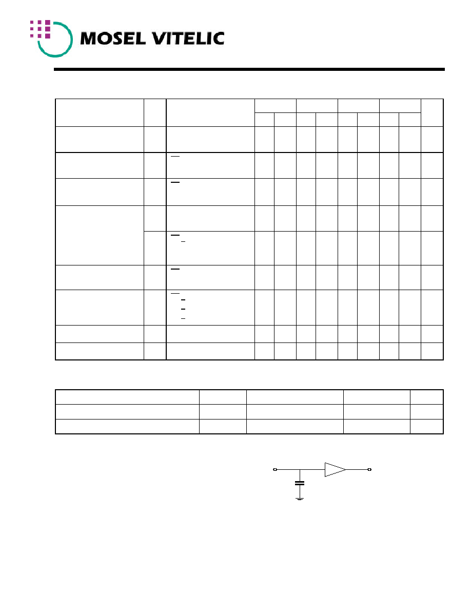
AC Test Conditions
Input Pulse Level
0.4V to 1.6V
Input Rise and Fall Time
5ns
Input and Output Timing
Reference Level
1.0V
Output Load Condition
70ns/85ns
C
L
= 30pf + 1TTL Load
Load for 100ns/120ns
C
L
= 100pf + 1TTL Load
C
L
*
Figure A. * Including Scope and Jig Capacitance
TTL
V62C1162048L(L)
DC Operating Characteristics
(V
cc
=1.8 to 2.2V, Gnd = 0V, T
A
= 0
0
C to +70
0
C / -40
0
C to 85
0
C)
Input Leakage Current
I
I
LI
I
V
cc
= Max,
V
in
= Gnd to V
cc
-
1
-
1
-
1
-
1
�
A
Output Leakage
Current
I
I
LO
I
CE = V
IH
or V
cc
=
Max,
V
OUT
=
Gnd to V
cc
-
1
-
1
-
1
-
1
�
A
Operating Power
Supply Current
I
CC
CE = V
IL
, V
IN
= V
IH
or
V
IL
,
I
OUT
=
0
-
5
-
5
-
5
-
5
mA
Average Operating
Current
I
CC1
I
OUT
=
0mA,
Min Cycle, 100% Duty
-
35
-
35
-
30
-
30
mA
I
CC2
CE < 0.2V
I
OUT
=
0mA,
Cycle Time=1
�
s, Duty=100%
-
3
-
3
-
3
-
3
mA
Standby Power Supply
Current (TTL Level)
I
SB
CE = V
IH
-
0.5
-
0.5
-
0.5
-
0.5
mA
Standby Power Supply
Current (CMOS Level)
I
SB1
CE > V
cc
- 0.2V
V
IN
< 0.2V or
V
IN
> V
cc
- 0.2V
L
-
-
10
2
-
-
10
2
-
-
10
2
-
-
10
2
�
A
�
A
Output Low Voltage
V
OL
I
OL
= 2 mA
-
0.4
-
0.4
-
0.4
-
0.4
V
Output High Voltage
V
OH
I
OH
= -1 mA
1.6
-
1.6
-
1.6
-
1.6
-
V
-70
-100
-120
Unit
Parameter
Sym
Test Conditions
Min Max Min Max Min Max Min Max
-85
4
Capacitance
(f = 1MHz, T
A
= 25
0
C)
Parameter*
Symbol
Test Condition
Max
Unit
Input Capacitance
C
in
V
in
= 0V
7
pF
I/O Capacitance
C
I/O
V
in
= V
out
= 0V
8
pF
* This parameter is guaranteed by device characterization and is not production tested.
REV. 1.
2 May 2001 V62C1162048L(L)
V62C1162048L(L)
Parameter
Sym
Unit
Note
Read Cycle Time
t
RC
70
-
85
-
100
-
120
-
ns
Address Access Time
t
AA
-
70
-
85
-
100
-
120
ns
Chip Enable Access Time
t
ACE
-
70
-
85
-
100
-
120
ns
Output Enable Access Time
t
OE
-
40
-
40
-
50
-
60
ns
Output
Hold from
Address Change
t
OH
10
-
10
-
10
-
10
-
ns
Chip Enable to Output in Low-Z
t
LZ
10
-
10
-
10
-
10
-
ns
4,5
Chip Disable to Output in High-Z
t
HZ
-
30
-
35
-
40
-
45
ns
3,4,5
Output Enable to Output in Low-Z
t
OLZ
5
-
5
-
5
-
5
-
ns
Output
Disable to
Output in High-Z
t
OHZ
-
25
-
30
-
35
-
40
ns
BLE, BHE Enable to Output in Low-Z
t
BLZ
5
-
5
-
5
-
5
-
ns
4,5
BLE, BHE Disable to Output in High-Z
t
BHZ
-
25
-
30
-
35
-
40
ns
3,4,5
BLE, BHE Access Time
t
BA
-
40
-
40
-
50
-
60
ns
Read Cycle
(9)
(V
cc
= 1.8 to 2.2V, Gnd = 0V, T
A
= 0
0
C to +70
0
C / -40
0
C to +85
0
C)
Write Cycle
(11)
(V
cc
= 1.8 to 2.2V, Gnd = 0V, T
A
= 0
0
C to +70
0
C / -40
0
C to +85
0
C)
Parameter
Symbol
Unit
Note
Write Cycle Time
t
WC
70
-
85
-
100
-
120
-
ns
Chip Enable to Write End
t
CW
60
-
70
-
80
-
90
-
ns
Address Setup to Write End
t
AW
60
-
70
-
80
-
90
-
ns
Address Setup Time
t
AS
0
-
0
-
0
-
0
-
ns
Write Pulse Width
t
WP
50
-
60
-
70
-
80
-
ns
Write Recovery Time
t
WR
0
-
0
-
0
-
0
-
ns
Data Valid to Write End
t
DW
30
-
35
-
40
-
45
-
ns
Data Hold Time
t
DH
0
-
0
-
0
-
0
-
ns
Write Enable to Output in High-Z
t
WHZ
-
30
-
35
-
40
-
45
ns
Output Active from Write End
t
OW
5
-
5
-
5
-
5
-
ns
BLE, BHE Setup to Write End
t
BW
60
-
70
-
80
-
90
-
ns
Min Max Min Max Min Max Min Max
-70
-85
-100
-120
5
Min Max Min Max Min Max Min Max
-70
-85
-100
-120
REV. 1.
2 May 2001 V62C1162048L(L)