
1
2
3
4
5
6
7
8
9
16
15
14
13
12
11
10
A
8
A
9
A
11
A
13
WE
CE
2
A
15
Vcc
NC
A
16
A
14
A
12
A
7
A
6
A
5
A
4
32
31
30
29
28
27
26
25
24
17
18
19
20
21
22
23
CE1
A
10
OE
I/O
8
I/O
7
I/O
6
I/O
5
I/O
4
GND
I/O
3
I/O
2
I/O
1
A
0
A
1
A
2
A
3
1024
X
1024
ROW DECODER
SENSE AMP
INPUT BUFFER
COLUMN DECODER
CONTROL
CIRCUIT
I/O
7
I/O
0
OE
WE
CE1
CE2
A
9
A
10
A
11
A
12
A
13
A
14
A
15
A
16
A
8
A
7
A
6
A
5
A
4
A
3
A
2
A
1
A
0
V62C1801024L(L)
Ultra Low Power
128K x 8 CMOS SRAM
Features
� Ultra Low-power consumption
- Active: 20mA at 70ns
- Stand-by: 5
�
A
(CMOS input/output)
1
�
A
CMOS input/output, L version
� Single +1.8V to 2.2V Power Supply
� Equal access and cycle time
� 70/85/100/150 ns access time
� Easy memory expansion with CE1 , CE2
and OE inputs
� 1.0V data retention mode
� TTL compatible, Tri-state input/output
� Automatic power-down when deselected
Functional Description
The V62C1801024L is a low power CMOS Static RAM or-
ganized as 131,072 words by 8 bits. Easy memory expansion
is provided by an active LOW CE1 , an active HIGH CE2, an
active LOW OE, and Tri-state I/O's. This device has an a-
utomatic power-down mode feature when deselected.
Writing to the device is accomplished by taking Chip E-
nable 1 (CE1 ) with Write Enable (WE) LOW, and Chip Ena-
ble 2 (CE2) HIGH. Reading from the device is performed by
taking Chip Enable 1 (CE1) with Output Enable (OE)
LOW while Write Enable (WE ) and Chip Enable 2 (CE2)
is HIGH. The I/O pins are placed in a high-impedance st-
ate when the device is deselected: the outputs are disabled
during a write cycle.
The V62C1801024LL comes with a 1V data retention feature
and Lower Standby Power. The V62C1801024L is available in
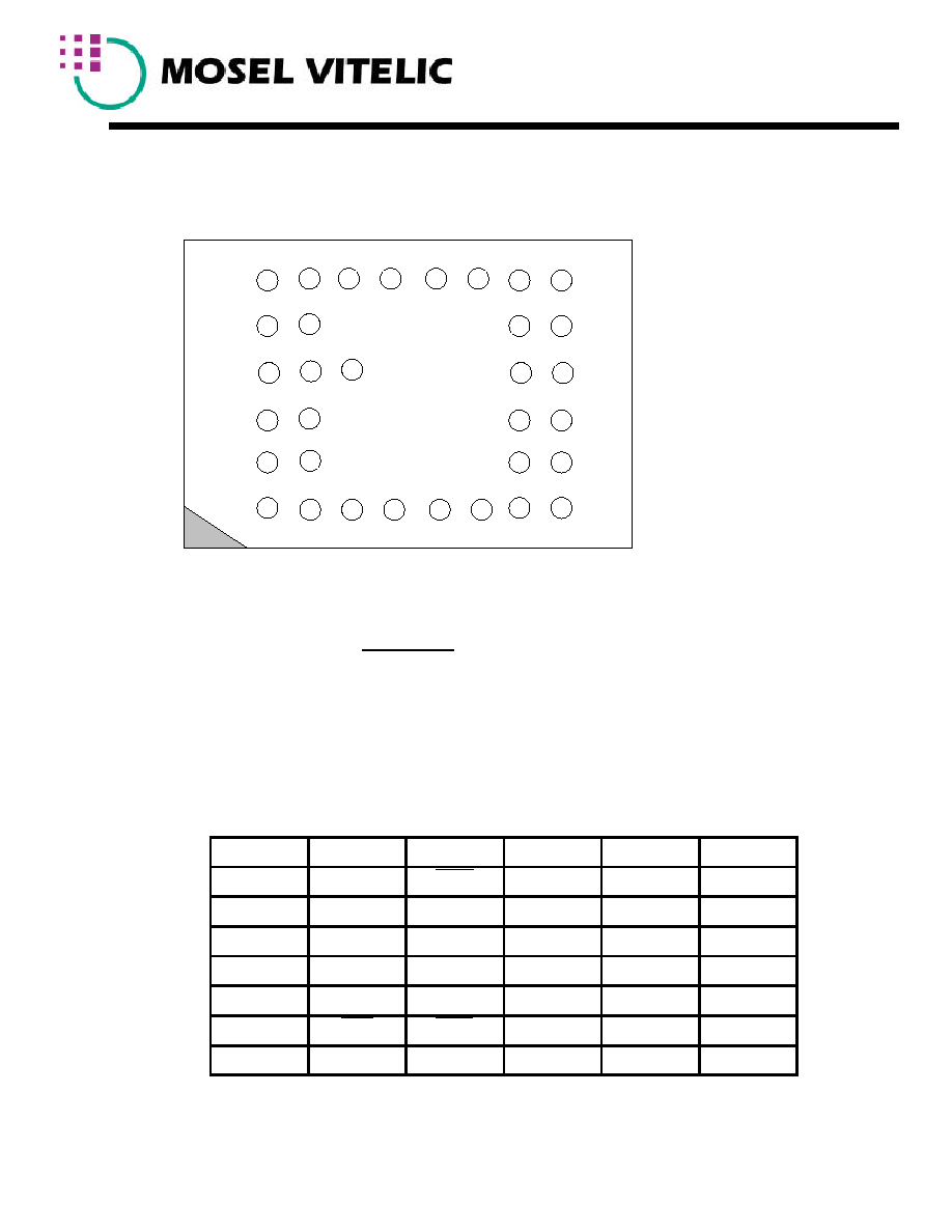
a 32-pin 8 x 20 mm TSOP1 / STSOP / 48-fpBGA packages.
32-Pin TSOP1 / STSOP
(See next page)
Logic Block Diagram
1024
X
1024
ROW DECODER
SENSE AMP
INPUT BUFFER
COLUMN DECODER
CONTROL
CIRCUIT
I/O8
I/O1
OE
WE
CE1
CE2
A
10
A
11
A
12
A
13
A
14
A
15
A
16
A
8
A
7
A
6
A
5
A
4
A
3
A
2
A
1
A
0
A
9
REV. 1.
1 April 2001 V62C1801024L(L)
1
V62C1801024L(L)
2
Top View
48-CSP Ball-Grid Array package (shading indicates no ball)
1
2
3
4
5
6
A
A
0
A
1
CE2
A
3
A
6
A
8
B
I/O
4
A
2
WE
A
4
A
7
I/O
0
C
I/O
5
NC
NC
A
5
NC
I/O
1
D
V
SS
NC
NC
NC
NC
V
DD
E
V
DD
NC
NC
NC
NC
V
SS
F
I/O
6
NC
NC
NC
NC
I/O
2
G
I/O
7
OE
CE
1
A
16
A
15
I/O
3
H
A
9
A
10
A
11
A
12
A
13
A
14
MOSEL VITELIC V62C1801024L(L)B
TOP VIEW
6
5
4
3
2
1
A B C D E F G H
REV. 1.
1 April 2001 V62C1801024L(L)

V62C1801024L(L)
Absolute Maximum Ratings *
* Note: Stresses greater than those listed above Absolute Maximum Ratings may cause permanent damage to the device. This is a stress rat-
ing only and functional operation of the device at these or any conditions outside those indicated in the operational sections of this specifica-
tion is not implied. Exposure to Absolute Maximum Rating conditions for extended periods may affect reliability.
Parameter
Symbol
Minimum
Maximum
Unit
Voltage on Any Pin Relative to Gnd
Vt
-0.5
4.6
V
Power Dissipation
P
T
-
1.0
W
Storage Temperature (Plastic)
Tstg
-55
+150
0
C
Temperature Under Bias
Tbias
-40
+85
0
C
Truth Table
* Key: X = Don't Care, L = Low, H = High
CE1
CE2
WE
OE
Data
Mode
H
X
X
X
High-Z
Standby
X
L
X
X
High-Z
Standby
L
H
H
L
Data Out
Active, Read
L
H
H
H
High-Z
Active, Output Disable
L
H
L
X
Data In
Active, Write
3
Recommended Operating Conditions
(T
A
= 0
0
C to +70
0
C / -40
0
C to 85
0
C
**
)
* V
IL
min = -1.0V for pulse width less than t
RC
/2.
** For Industrial Temperature.
Parameter
Symbol
Min
Typ
Max
Unit
V
CC
1.8
2.0
2.2
V
Gnd
0.0
0.0
0.0
V
V
IH
1.6
-
V
CC
+ 0.2
V
V
IL
-0.5*
-
0.4
V
Supply Voltage
Input Voltage
REV. 1.
1 April 2001 V62C1801024L(L)
AC Test Conditions
Input Pulse Level
0.4V to 1.6V
Input Rise and Fall Time
5ns
Input and Output Timing
Reference Level
50% of input level
(V
IL
+ V
IH
)/2
Output Load Condition
70ns/85 ns
C
L
= 30pf + 1TTL Load
Load 100ns/150 ns
C
L
= 100pf + 1TTL Load
C
L
*
Figure A. * Including Scope and Jig Capacitance
TTL
V62C1801024L(L)
DC Operating Characteristics
(V
cc
= 1.8 to 2.2V, Gnd = 0V, T
A
= 0
0
C to +70
0
C / -40
0
C to 85
0
C)
Input Leakage Current
I
I
LI
V
cc
= Max,
V
in
= Gnd to V
cc
-
1
-
1
-
1
-
1
�
A
Output Leakage
Current
I
I
LO
CE1 = V
IH
or CE2 = V
IL
V
cc
=
Max,
V
OUT
=
Gnd to V
cc
-
1
-
1
-
1
-
1
�
A
Operating Power
Supply Current
I
CC
CE1 = V
IL
, CE2 = V
IH
V
IN
= V
IH
or
V
IL
,
I
OUT
=
0
mA
-
3
-
3
-
3
-
3
mA
Average Operating
Current
I
CC1
CE1 = V
IL
, CE2 = V
IH
I
OUT
=
0mA,
Min Cycle, 100% Duty
-
25
-
20
-
15
-
15
mA
I
CC2
CE1 = 0.2V,
CE2 = V
cc
- 0.2V
I
OUT
=
0mA,
Cycle Time=1
�
s, 100% Duty
-
3
-
3
-
3
-
3
mA
Standby Power Supply
Current (TTL Level)
I
SB
CE1 = V
IH
or CE2 = V
IL
-
0.5
-
0.5
-
0.5
-
0.5
mA
Standby Power Supply
Current (CMOS Level)
I
SB1
CE1 > V
cc
- 0.2V
or
L
CE2 < 0.2V, f = 0
V
IN
< 0.2V or
V
IN
> V
cc
- 0.2V
LL
-
-
5
1
-
-
5
1
-
-
5
1
-
-
5
1
�
A
�
A
Output Low Voltage
V
OL
I
OL
= 2 mA - 0.4 - 0.4 - 0.4 - 0.4 V
Output High Voltage
V
OH
I
OH
= -1 mA
1.6
-
1.6
-
1.6
-
1.6
-
V
-70
-100
-150
Unit
Parameter
Sym
Test Conditions
Min Max Min Max Min Max Min Max
-85
4
Capacitance
(f = 1MHz, T
A
= 25
0
C)
Parameter*
Symbol
Test Condition
Max
Unit
Input Capacitance
C
in
V
in
= 0V
7
pF
I/O Capacitance
C
I/O
V
in
= V
out
= 0V
8
pF
* This parameter is guaranteed by device characterization and is not production tested.
REV. 1.
1 April 2001 V62C1801024L(L)
V62C1801024L(L)
Parameter
Symbol
Unit
Note
Read Cycle Time
t
RC
70
-
85
-
100
-
150
-
ns
Address Access Time
t
AA
-
70
-
85
-
100
-
150
ns
Chip Enable Access Time
t
ACE
-
70
-
85
-
100
-
150
ns
Output Enable Access Time
t
OE
-
40
-
40
-
50
-
70
ns
Output
Hold from
Address Change
t
OH
10
-
10
-
10
-
10
-
ns
Chip Enable to Output in Low-Z
t
CLZ
10
-
10
-
10
-
10
-
ns
4,5
Chip Disable to Output in High-Z
t
CHZ
-
30
-
35
-
40
-
50
ns
4,5
Output Enable to Output in Low-Z
t
OLZ
5
-
5
-
5
-
5
-
ns
4,5
Output
Disable to
Output in High-Z
t
OHZ
-
25
-
30
-
35
-
40
ns
4,5
Power-Up Time
t
PU
0
-
0
-
0
-
0
-
ns
5
Power-Down Time
t
PD
-
70
-
85
-
100
-
150
ns
5
Read Cycle
(3,9)
(V
cc
= 1.8 to 2.2V, Gnd = 0V, T
A
= 0
0
C to +70
0
C / -40
0
C to +85
0
C)
Write Cycle
(3,11)
(V
cc
= 1.8 to 2.2V, Gnd = 0V, T
A
= 0
0
C to +70
0
C / -40
0
C to +85
0
C)
Parameter
Symbol
Unit
Note
Write Cycle Time
t
WC
70
-
85
-
100
-
150
-
ns
Chip Enable to Write End
t
CW
60
-
70
-
80
-
120
-
ns
Address Setup to Write End
t
AW
60
-
70
-
80
-
120
-
ns
Address Setup Time
t
AS
0
-
0
-
0
-
0
-
ns
Write Pulse Width
t
WP
50
-
60
-
70
-
100
-
ns
Write Recovering Time
t
WR
0
-
0
-
0
-
0
-
ns
Data Valid to Write End
t
DW
30
-
35
-
40
-
60
-
ns
Data Hold Time
t
DH
0
-
0
-
0
-
0
-
ns
Write Enable to Output in High-Z
t
WZ
-
30
-
35
-
40
-
50
ns
4,5
Output Active from Write End
t
OW
5
-
5
-
5
-
5
-
ns
4,5
Min Max Min Max Min Max Min Max
-70
-85
-100
5
Min Max Min Max Min Max Min Max
-70
-85
-100
-150
-150
REV. 1.
1 April 2001 V62C1801024L(L)