MOSEL VITELIC
1
V62C1804096
512K X 8, CMOS STATIC RAM
PRELIMINARY
V62C1804096 Rev. 1.0 October 2001
Features
s
High-speed: 85, 100 ns
s
Ultra low standby current of 2µA (max.)
s
Fully static operation
s
All inputs and outputs directly compatible
s
Three state outputs
s
Ultra low data retention current (V
CC
= 1.0V)
s
Operating voltage: 1.8V≠2.3V
s
Packages
≠ 36-Ball CSP BGA (8mm x 10mm)
Description
The V62C1804096 is a very low power CMOS
static RAM organized as 524,288 words by 8 bits.
Easy memory expansion is provided by an active
LOW CE1, and active HIGH CE2, an active LOW
OE, and three static I/O's. This device has an
a u to m a ti c p o w e r -d o w n m o d e f e a tu r e w h e n
deselected.
Device Usage Chart
Operating
Temperature
Range
Package
Outline
Access Time (ns)
Power
Temperature
Mark
B
85
100
L
LL
0∞C to 70 ∞C
∑
∑
∑
∑
∑
Blank
≠40∞C to +85∞C
∑
∑
∑
∑
I
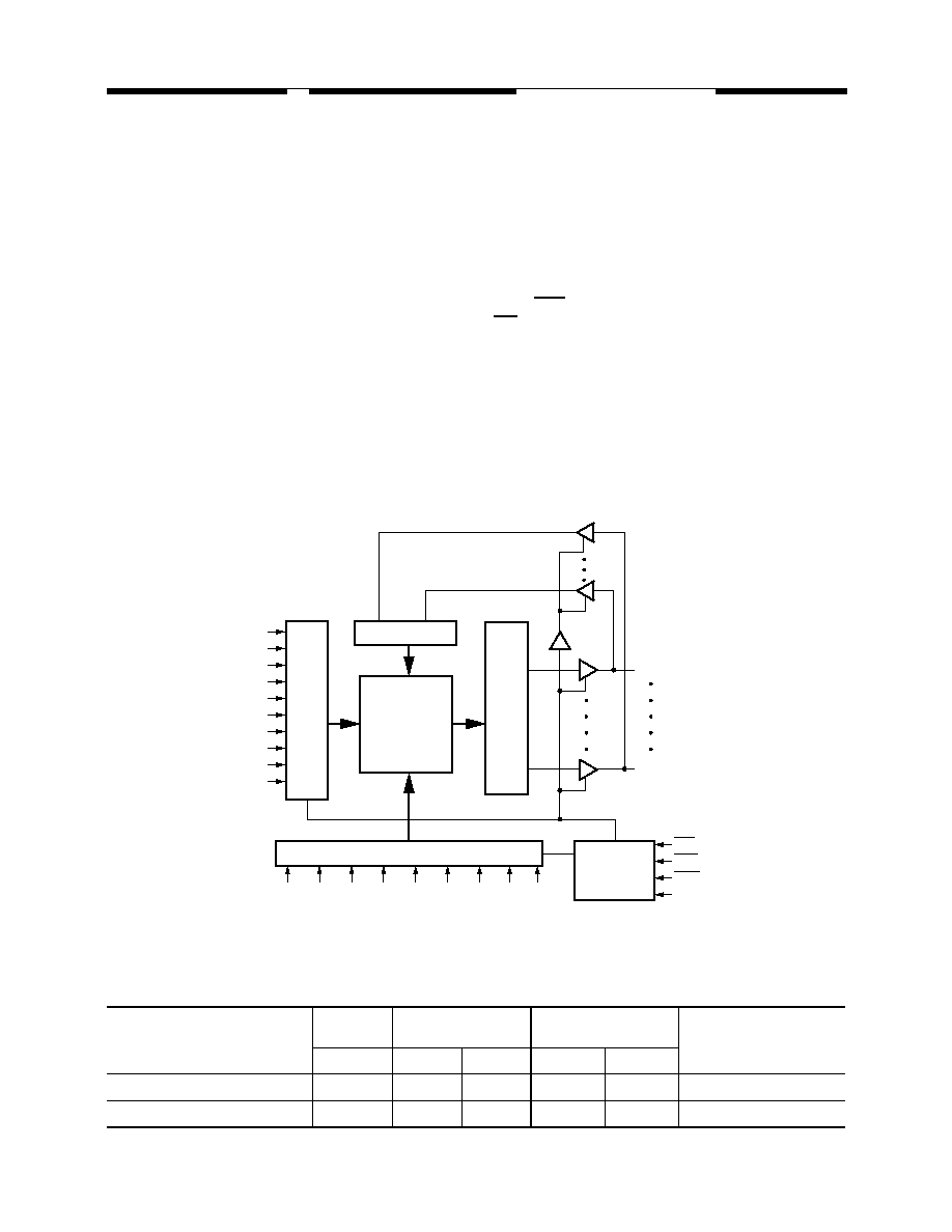
Functional Block Diagram
Row Decoder
Sense Amp
1024
x
4096
Column Decoder
Input Buffer
Control
Circuit
A
0
A
1
A
2
A
3
A
4
A
5
A
6
A
7
A
8
A
9
A
10
A
11
A
12
A
13
A
14
A
15
A
16
I/O1
I/O
8
OE
WE
CE1
CE2
A
17
A
18
2
V62C1804096 Rev. 1.0 October 2001
MOSEL VITELIC
V62C1804096
Pin Descriptions
A
0
≠A
18
Address Inputs
These 19 address inputs select one of the 512K x 8
bit segments in the RAM.
CE
1
, CE
2
Chip Enable Inputs
CE
1
is active LOW and CE
2
is active HIGH. Both
chip enables must be active to read from or write to
the device. If either chip enable is not active, the
device is deselected and is in a standby power
mode. The I/O pins will be in the high-impedance
state when deselected.
OE
Output Enable Input
The Output Enable input is active LOW. With chip
enabled, when OE is LOW and WE HIGH, data of
the selected memory location will be available on
the I/O pins. When OE is HIGH, the I/O pins will be
in the high impedance state.
WE
Write Enable Input
The write enable input is active LOW and controls
read and write operations. With the chip enabled,
when WE is HIGH and OE is LOW, output data will
be present at the I/O pins; when WE is LOW and
OE is HIGH, the data present on the I/O pins will be
written into the selected memory locations.
I/O
1
≠I/O
8
Data Input and Data Output Ports
These 8 bidirectional ports are used to read data
from and write data into the RAM.
V
CC
Power Supply
GND
Ground
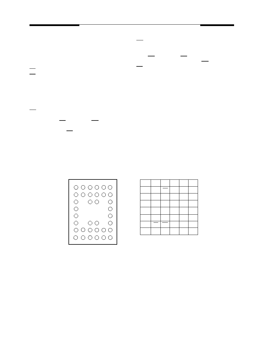
Pin Configurations (Top View)
36 BGA
A
1
2
3
4
5
6
1
Note: NC means no connect.
NB means no ball.
2
TOP VIEW
TOP VIEW
3
4
5
6
B
C
D
E
F
G
H
A
A0
I/O5
I/O6
B
C
D
E
F
G
H
VSS
VCC
I/O7
I/O8
A9
A1
A2
NB
NB
NB
NB
OE
A10
CE2
WE
NC
NB
NB
A18
CE1
A11
A3
A4
A5
NB
NB
A17
A16
A12
A6
A7
NB
NB
NB
NB
A15
A13
A8
I/O1
I/O2
VCC
VSS
I/O3
I/O4
A14
MOSEL VITELIC
V62C1804096
3
V62C1804096 Rev. 1.0 October 2001
Part Number Information
Absolute Maximum Ratings
(1)
NOTE:
1.
Stresses greater than those listed under "Absolute Maximum Ratings" may cause permanent damage to the device. This is a stress
rating only and functional operation of the device at these or any other conditions above those indicated in the operational sections
of this specification is not implied. Exposure to absolute maximum rating conditions for extended periods may affect reliability.
Symbol
Parameter
Commercial
Industrial
Units
V
CC
Supply Voltage
-0.5 to + V
CC
+ 0.5
-0.5 to + V
CC
+ 0.5
V
V
N
Input Voltage
-0.5 to + V
CC
+ 0.5
-0.5 to + V
CC
+ 0.5
V
V
DQ
Input/Output Voltage Applied
V
CC
+ 0.3
V
CC
+ 0.3
V
T
BIAS
Temperature Under Bias
-10 to +125
-65 to +135
∞C
T
STG
Storage Temperature
-55 to +125
-65 to +150
∞C
SRAM
FAMILY
C = CMOS PROCESS
62 = STANDARD
18 = 1.8V≠2.3V
OPERATING
VOLTAGE
4096K
ORGANIZATION
PKG
SPEED
62
C
8
18
4096
≠
MOSEL-VITELIC
MANUFACTURED
V
8 = 8-bit
85 ns
100 ns
TEMP.
BLANK = 0
∞
C to 70
∞
C
I = -40
∞
C to +85
∞
C
L = LOW POWER
LL = LOW LOW POWER
T = TSOP STANDARD
B = BGA
DENSITY
PWR.
1
1
80
80
Capacitance*
T
A
= 25∞C, f = 1.0MHz
NOTE:
1.
This parameter is guaranteed and not tested.
Truth Table
NOTE:
X = Don't Care, L = LOW, H = HIGH
Symbol
Parameter
Conditions
Max.
Unit
C
IN
Input Capacitance
V
IN
= 0V
6
pF
C
OUT
Output Capacitance
V
I/O
= 0V
8
pF
Mode
CE
1
CE
2
OE
WE
I/O
Operation
Standby
H
X
X
X
High Z
Standby
X
L
X
X
High Z
Output Disable
L
H
H
H
High Z
Read
L
H
L
H
D
OUT
Write
L
H
X
L
D
IN
4
V62C1804096 Rev. 1.0 October 2001
MOSEL VITELIC
V62C1804096
DC Electrical Characteristics
(over all temperature ranges, V
CC
= 1.8V≠2.3V)
NOTES:
1.
These are absolute values with respect to device ground and all overshoots due to system or tester noise are included.
2.
V
IL
(Min.) = -3.0V for pulse width < t
RC
/2.
3.
Maximum value.
Symbol
Parameter
Test Conditions
Min.
Typ.
Max.
Units
V
IL
Input LOW Voltage
(1,2)
-0.3
--
0.4
V
V
IH
Input HIGH Voltage
(1)
1.6
--
V
CC
+0.3
V
I
IL
Input Leakage Current
V
CC
= Max, V
IN
= 0V to V
CC
--
--
1
µA
I
OL
Output Leakage Current
V
CC
= Max, CE
1
= V
IH
, V
OUT
= 0V to V
CC
--
--
1
µA
V
OL
Output LOW Voltage
V
CC
= Min, I
OL
= 2mA
--
--
0.4
V
V
OH
Output HIGH Voltage
V
CC
= Min, I
OH
= -0.5mA
V
CC
≠0.4
--
--
V
Symbol
Parameter
Comm.
(3)
Ind.
(3)
Units
I
CC1
Average Operating Current, CE
1
= V
IL
, CE
2
= V
CC
≠ 0.2, Output Open,
V
CC
= Max.
f = fmax
25
30
mA
f = 1 MHz
2
3
I
SB
TTL Standby Current
CE
1
>=V
IH
, CE
2
<= V
IL
, V
CC
= Max., f = 0
L
0.4
0.5
mA
LL
0.3
0.3
I
SB1
CMOS Standby Current, CE
1
S V
CC
≠ 0.2V, CE
2
0.2V,
V
IN
>= V
CC
≠ 0.2V or V
IN
<=0.2V, V
CC
= Max., f = 0
L
5
7
µA
LL
2
3
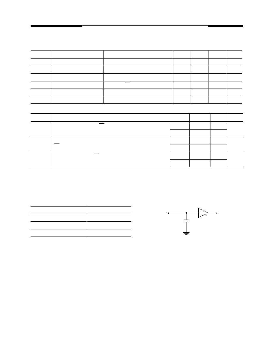
AC Test Conditions
AC Test Loads and Waveforms
Input Pulse Levels
0 to 1.6V
Input Rise and Fall Times
5 ns
Timing Reference Levels
0.9V
Output Load
see below
* Includes scope and jig capacitance
C
L
= 30pF + 1TTL Load
C
L
*
TTL
MOSEL VITELIC
V62C1804096
5
V62C1804096 Rev. 1.0 October 2001
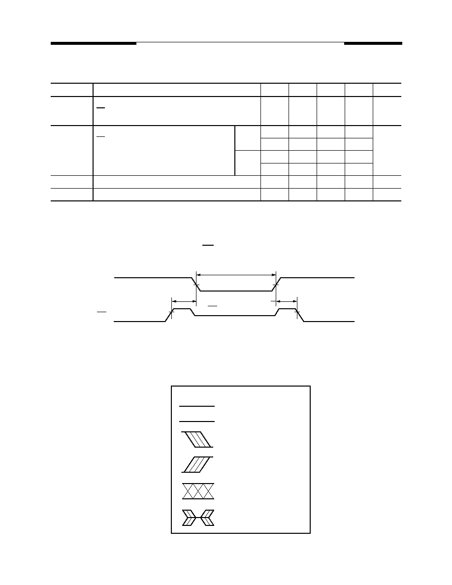
Data Retention Characteristics
NOTES:
1.
t
RC
= Read Cycle Time
2.
T
A
= +25
∞
C.
Low V
CC
Data Retention Waveform (1) (CE
1
Controlled)
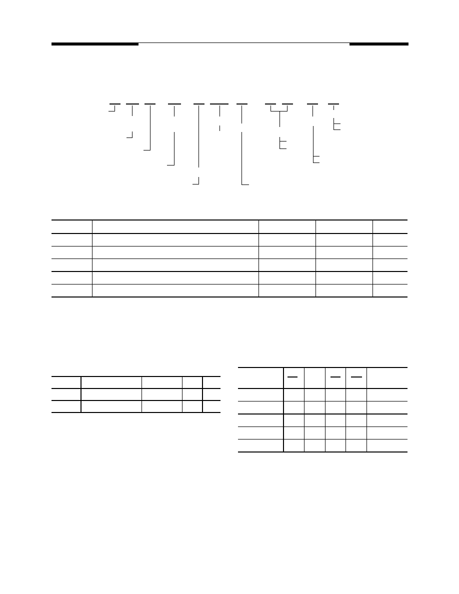
Key to Switching Waveforms
Symbol
Parameter
Power
Min.
Typ.
(2)
Max.
Units
V
DR
V
CC
for Data Retention
CE
1
V
CC
≠ 0.2V, CE
2
< 0.2V, V
IN
V
CC
≠ 0.2V,
or V
IN
0.2V
1.0
--
2.3
V
I
CCDR
Data Retention Current
CE
1
V
DR
≠ 0.2V, CE
2
< 0.2V, V
IN
V
CC
≠ 0.2V,
or V
IN
0.2V, V
DR
= 1.0V
Com'l
L
--
1
3
µ
A
LL
--
0.5
1.5
Ind.
L
--
--
5
LL
--
--
2
t
CDR
Chip Deselect to Data Retention Time
0
--
--
ns
t
R
Operation Recovery Time (see Retention Waveform)
t
RC
(1)
--
--
ns
V
CC
Data Retention Mode
CE
1
V
CC
≠ 0.2V
CE
1
1.6V
1.6V
1.8V
t
CDR
t
R
V
DR
1V
1.8V
WAVEFORM
INPUTS
OUTPUTS
MUST BE
STEADY
WILL BE
STEADY
MAY CHANGE
FROM H TO L
WILL BE
CHANGING
FROM H TO L
MAY CHANGE
FROM L TO H
WILL BE
CHANGING
FROM L TO H
DON'T CARE:
ANY CHANGE
PERMITTED
CHANGING:
STATE
UNKNOWN
DOES NOT
APPLY
CENTER
LINE IS HIGH
IMPEDANCE
"OFF" STATE