MOSEL VITELIC
1
V82648R04SATG
2.5 VOLT 8M x 64 HIGH PERFORMANCE
UNBUFFERED DDR SDRAM MODULE
PRELIMINARY
V82648R04SATG Rev. 1.0 February 2001
Features
s
184 Pin Unbuffered 8,388,608 x 64 bit
Organization SDRAM Modules
s
Utilizes High Performance 8M x 16 SDRAM in
TSOPII-66 Packages
s
Single +2.5V (± 0.2V) Power Supply
s
Programmable CAS Latency, Burst Length, and
Wrap Sequence (Sequential & Interleave)
s
Auto Refresh (CBR) and Self Refresh
s
All Inputs, Outputs are SSTL-2 Compatible
s
4096 Refresh Cycles every 64 ms
s
Serial Present Detect (SPD)
s
SDRAM Performance
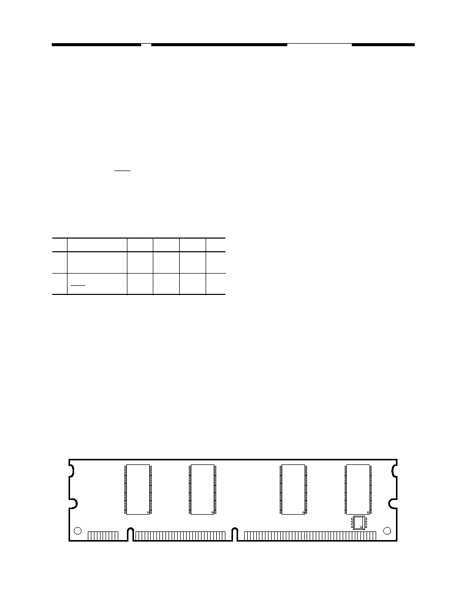
Description
The V82648R04SATG memory module is orga-
nized 8,388,608 x 64 bits in a 184 pin memory mod-
ule. The 8M x 64 memory module uses 4 Mosel-
Vitelic 8M x 16 SDRAM. The x64 modules are ideal
for use in high performance computer systems
where increased memory density and fast access
times are required.
Component Used
-7
-75
-8
Units
t
CK
Clock Frequency
(max.)
143
(PC266A)
133
(PC266B)
125
(PC200)
MHz
t
AC
Clock Access Time
CAS Latency = 2.5
7
75
8
ns
2
MOSEL VITELIC
V82648R04SATG
V82648R04SATG Rev. 1.0 February 2001
Part Number Information
DDR
2.5V
8
MOSEL-VITELIC
MANUFACTURED
V
184 PIN UNBUFFERED
DIMM X 16 COMPONENT
R
REFRESH
RATE 4K
0
2
DEPTH
8
4 BANKS
4
TSOP
WIDTH
64
SSTL-2
S
GOLD
G
T
Component Rev
A
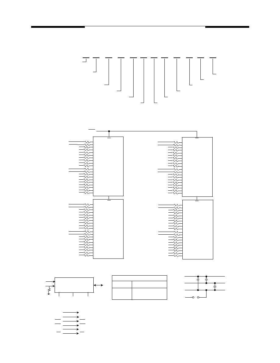
Block Diagram
CS0
Serial PD
A0
A1
A2
SA0
SA1
SA2
SCL
WP
BA0-BA1 BA0-BA1 : SDRAMs D0 - D3
A0 - A13 A0 - A13 : SDRAMs D0 - D3
RAS RAS : SDRAMs D0 - D3
CAS CAS : SDRAMs D0 - D3
CKE0 CKE : SDRAMs D0 - D3
WE WE : SDRAMs D0 - D3
Clock Wiring
Clock Input
SDRAMs
*CK0,/CK0
*CK1,/CK1
*CK2,/CK2
NC
2 SDRAMs
2 SDRAMs
Notes:
1. DQ-to-I/O wiring is shown as recommended
but may be changed.
2. DQ/DQS/DM/CKE/S relationships must be
maintained as shown.
3. DQ,DQS, DM/DQS resistors : 22 Ohms.
4. VDDID strap connections
(for memory device VDD, VDDQ) :
Strap out :(open) : VDD=VDDQ
Strap In (Vss) : VDD
VDDQ
* Wire per clock loading table/wiring diagrams
D0
CS
LDQS
LDM
I/O 6
I/O 4
I/O 1
I/O 3
I/O 2
I/O 0
I/O 5
I/O 7
UDQS
UDM
I/O 8
I/O 10
I/O 15
I/O 13
I/O 12
I/O 14
I/O 11
I/O 9
DQ8
DQ9
DQ10
DQ11
DQ12
DQ13
DQ14
DQ15
D M 1
D Q S 1
DQ0
DQ1
DQ2
DQ3
DQ4
DQ5
DQ6
DQ7
D M 0
D Q S 0
D1
LDQS
LDM
I/O 6
I/O 4
I/O 1
I/O 3
I/O 2
I/O 0
I/O 5
I/O 7
UDQS
UDM
I/O 8
I/O 10
I/O 15
I/O 13
I/O 12
I/O 14
I/O 11
I/O 9
DQ24
DQ25
DQ26
DQ27
DQ28
DQ29
DQ30
DQ31
D M 3
D Q S 3
DQ16
DQ17
DQ18
DQ19
DQ20
DQ21
DQ22
DQ23
D M 2
D Q S 2
D2
LDQS
LDM
I/O 6
I/O 4
I/O 1
I/O 3
I/O 2
I/O 0
I/O 5
I/O 7
UDQS
UDM
I/O 8
I/O 10
I/O 15
I/O 13
I/O 12
I/O 14
I/O 11
I/O 9
DQ40
DQ41
DQ42
DQ43
DQ44
DQ45
DQ46
DQ47
D M 5
D Q S 5
DQ32
DQ33
DQ34
DQ35
DQ36
DQ37
DQ38
DQ39
D M 4
D Q S 4
D3
LDQS
LDM
I/O 6
I/O 4
I/O 1
I/O 3
I/O 2
I/O 0
I/O 5
I/O 7
UDQS
UDM
I/O 8
I/O 10
I/O 15
I/O 13
I/O 12
I/O 14
I/O 11
I/O 9
DQ56
DQ57
DQ58
DQ59
DQ60
DQ61
DQ62
DQ63
D M 7
D Q S 7
DQ48
DQ49
DQ50
DQ51
DQ52
DQ53
DQ54
DQ55
D M 6
D Q S 6
47K
SDA
VDDVDDQ
VREF
Vss
D0 - D3
D0 - D3
D0 - D3
VDDID
CS
CS
CS
MOSEL VITELIC
V82648R04SATG
3
V82648R04SATG Rev. 1.0 February 2001
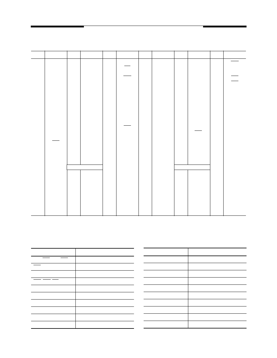
Pin Configurations (Front Side/Back Side)
Notes:
* These pins are not used in this module.
Pin
Front
Pin
Front
Pin
Front
Pin
Back
Pin
Back
Pin
Back
1
2
3
4
5
6
7
8
9
10
11
12
13
14
15
16
17
18
19
20
21
22
23
24
25
26
27
28
29
30
31
VREF
DQ0
VSS
DQ1
DQS0
DQ2
VDD
DQ3
NC
NC
VSS
DQ8
DQ9
DQS1
VDDQ
CK1
CK1
VSS
DQ10
DQ11
CKE0
VDDQ
DQ16
DQ17
DQS2
VSS
A9
DQ18
A7
VDDQ
DQ19
32
33
34
35
36
37
38
39
40
41
42
43
44
45
46
47
48
49
50
51
52
53
54
55
56
57
58
59
60
61
A5
DQ24
VSS
DQ25
DQS3
A4
VDD
DQ26
DQ27
A2
Vss
A1
CB0*
CB1*
VDD
DQS8*
A0
CB2*
VSS
CB3*
BA1
Key
DQ32
VDDQ
DQ33
DQS4
DQ34
VSS
BA0
DQ35
DQ40
62
63
64
65
66
67
68
69
70
71
72
73
74
75
76
77
78
79
80
81
82
83
84
85
86
87
88
89
90
91
92
VDDQ
WE
DQ41
CAS
VSS
DQS5
DQ42
DQ43
VDD
NC
DQ48
DQ49
VSS
CK2
CK2
VDDQ
DQS6
DQ50
DQ51
VSS
VDDID
DQ56
DQ57
VDD
DQS7
DQ58
DQ59
VSS
NC
SDA
SCL
93
94
95
96
97
98
99
100
101
102
103
104
105
106
107
108
109
110
111
112
113
114
115
116
117
118
119
120
121
122
123
VSS
DQ4
DQ5
VDDQ
DM0
DQ6
DQ7
VSS
NC
NC
A13*
VDDQ
DQ12
DQ13
DM1
VDD
DQ14
DQ15
CKE1
VDDQ
BA2*
DQ20
A12*
VSS
DQ21
A11
DM2
VDD
DQ22
A8
DQ23
124
125
126
127
128
129
130
131
132
133
134
135
136
137
138
139
140
141
142
143
144
145
146
147
148
149
150
151
152
153
VSS
A6
DQ28
DQ29
VDDQ
DM3
A3
DQ30
VSS
DQ31
CB4*
CB5*
VDDQ
CK0*
CK0*
VSS
DM8*
A10
CB6*
VDDQ
CB7*
key
VSS
DQ36
DQ37
VDD
DM4
DQ38
DQ39
VSS
DQ44
154
155
156
157
158
159
160
161
162
163
164
165
166
167
168
169
170
171
172
173
174
175
176
177
178
179
180
181
182
183
184
RAS
DQ45
VDDQ
CS0
CS1
DM5
VSS
DQ46
DQ47
NC
VDDQ
DQ52
DQ53
NC
VDD
DM6
DQ54
DQ55
VDDQ
NC
DQ60
DQ61
VSS
DM7
DQ62
DQ63
VDDQ
SA0
SA1
SA2
VDDSPD
Pin Names
Pin Pin
Description
CK1, CK1, CK2, CK2
Differential Clock Inputs
CS0
Chip Select Input
CKE0
Clock Enable Input
RAS, CAS, WE
Commend Sets Inputs
A0 ~ A11
Address
BA0, BA1
Bank Address
DQ0~DQ63 Data
Inputs/Outputs
DQS0~DQS7
Data Strobe Inputs/Outputs
DM0~DM7 Data-in
Mask
VDD Power
Supply
Key
Key
VDDQ
DQs Power Supply
VSS Ground
VREF
Reference Power Supply
VDDSPD
Power Supply for SPD
SA0~SA2 E
2
PROM Address Inputs
SCL E
2
PROM Clock
SDA E
2
PROM Data I/O
VDDID
VDD Identification Flag
DU
Do not Use
NC No
Connection
Pin Pin
Description
4
MOSEL VITELIC
V82648R04SATG
V82648R04SATG Rev. 1.0 February 2001
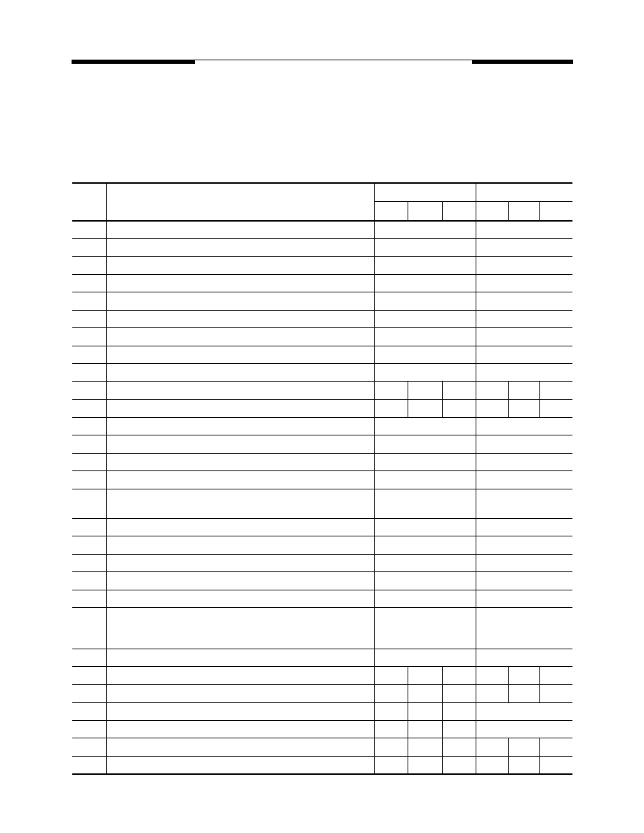
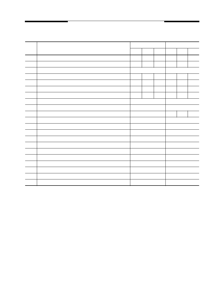
Serial Presence Detect Information
Bin Sort:
A
(PC266A @ CL = 2)
B
(PC266B @ CL = 2.5)
C
(PC200 @ CL = 2)
Byte #
Function described
Function Supported
Hex value
C B A C
B A
0
Defines # of Bytes written into serial memory at module manufacturer
128bytes
80h
1
Total # of Bytes of SPD memory device
256bytes
08h
2
Fundamental memory type
SDRAM DDR
07h
3
# of row address on this assembly
12
0Ch
4
# of column address on this assembly
9
09h
5
# of module Rows on this assembly
1 Bank
01h
6
Data width of this assembly
64 bits
40h
7
.........Data width of this assembly
-
00h
8
VDDQ and interface standard of this assembly
SSTL 2.5V
04h
9
DDR SDRAM cycle time at CAS Latency =2.5
8ns
7.5ns
7ns
80h
75h
70h
10
DDR SDRAM Access time from clock at CL=2.5
±0.8ns ±0.75n ±0.75n
80h
75h
75h
11
DIMM configuration type(Non-parity, Parity, ECC)
Non-parity, ECC
00h
12
Refresh rate & type
15.6us & Self refresh
80h
13
Primary DDR SDRAM width
x16
10h
14
Error checking DDR SDRAM data width
N/A
00h
15
Minimum clock delay for back-to-back random column
address
t
CCD
=1CLK 01h
16
DDR SDRAM device attributes : Burst lengths supported
2,4,8
0Eh
17
DDR SDRAM device attributes : # of banks on each DDR SDRAM
4 banks
04h
18
DDR SDRAM device attributes : CAS Latency supported
2,2.5
0Ch
19
DDR SDRAM device attributes : CS Latency
0CLK
01h
20
DDR SDRAM device attributes : WE Latency
1CLK
02h
21
DDR SDRAM module attributes
Registered address&
control inputs and On-card
DLL
20h
22
DDR SDRAM device attributes : General
+/-0.2V voltage tolerance
00h
23
DDR SDRAM cycle time at CL =2
10ns
10ns
7.5ns
A0h
A0h
75h
24
DDR SDRAM Access time from clock at CL =2
±0.8ns ±0.75n ±0.75
80h
75h
75h
25
DDR SDRAM cycle time at CL =1.5
-
-
-
00h
26
DDR SDRAM Access time from clock at CL =1.5
-
-
-
00h
27
Minimum row precharge time (=t
RP
)
20ns 20ns 20ns 50h 50h 50h
28
Minimum row activate to row active delay(=t
RRD
)
15ns 15ns 15ns 3Ch 3Ch 3Ch
MOSEL VITELIC
V82648R04SATG
5
V82648R04SATG Rev. 1.0 February 2001
29
Minimum RAS to CAS delay(=t
RCD
)
20ns 20ns 20ns 50h 50h 50h
30
Minimum active to precharge time(=t
RAS
)
48ns 48ns 45ns 30h 30h 2Dh
31
Module ROW density
64MB
10h
32
Command and address signal input setup time
1.1ns
0.9ns
0.9ns
B0h
90h
90h
33
Command and address signal input hold time
1.1ns
0.9ns
0.9ns
B0h
90h
90h
34
Data signal input setup time
0.6ns
0.5ns
0.5ns
60h
50h
50h
35
Data signal input hold time
0.6ns
0.5ns
0.5ns
60h
50h
50h
36-61
Superset information (may be used in future)
-
00h
62
SPD data revision code
Initial release
00h
63
Checksum for Bytes 0 ~ 62
-
17h
96h
63h
64
Manufacturer JEDEC ID code
Mosel Vitelic
40h
65 -71
....... Manufacturer JEDEC ID code
Mosel Vitelic
40h
72
Manufacturing location
01h
73-90
Module part number (ASCII)
V82648Y04SATG
91
Manufacturer revison code (For PCB)
0
00
92
Manufacturer revison code (For component)
0
00
93
Manufacturing date (Week)
-
-
94
Manufacturing date (Year)
-
-
95~98
Assembly serial #
-
-
99~127 Manufacturer specific data (may be used in future)
Undefined
00h
128~255 Open for customer use
Undefined
00h
Byte #
Function described
Function Supported
Hex value
C B A C
B A
Serial Presence Detect Information (cont.)