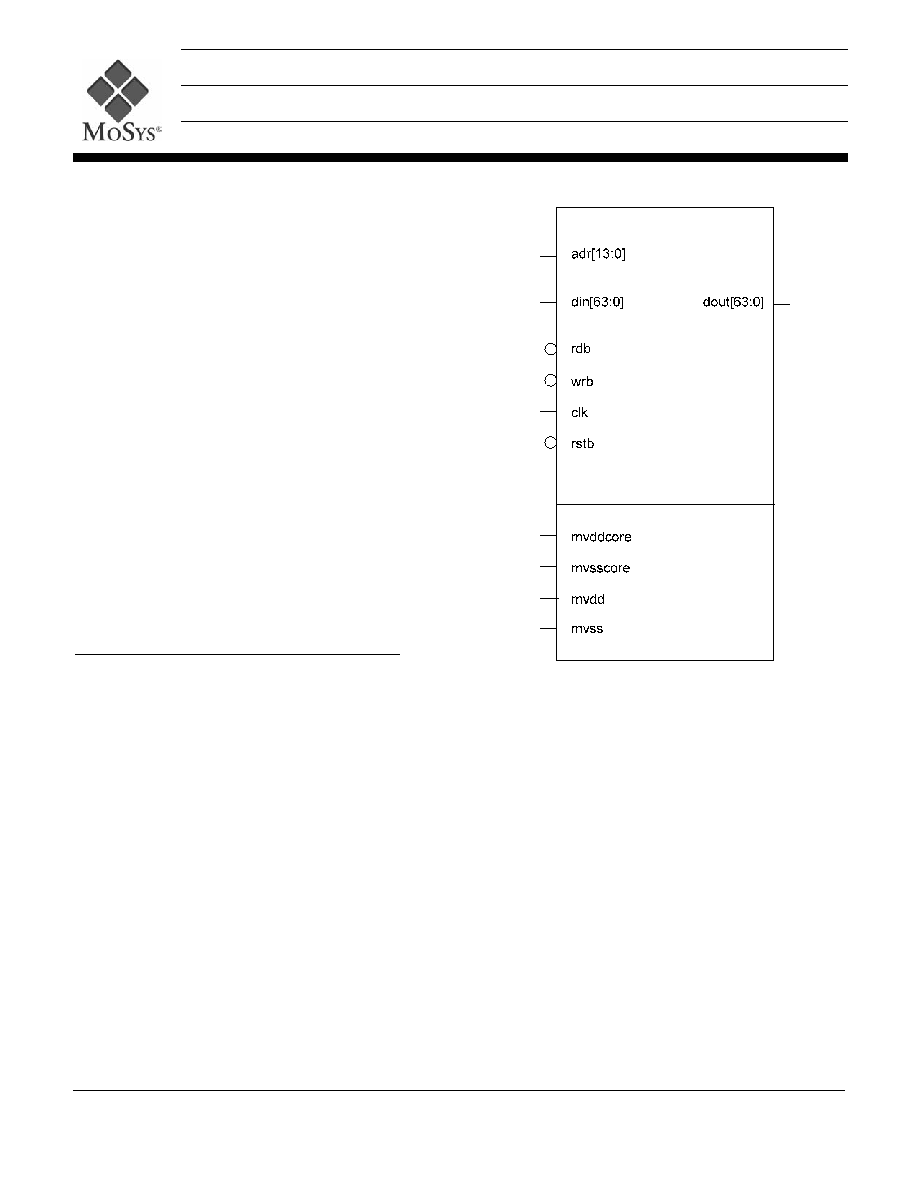
High Speed Pipelined 1-Mbit (16Kx64)
Standard 1T-SRAM
Æ
Embedded Memory Macro
M1T1HT25PZ64
M1T1HT25PZ64 Rev1_033
Page 1
© 2001 MoSys Inc., All Rights Reserved, 1020 Stewart Drive, Sunnyvale, CA 94085
∑
High Speed 1T-SRAM Standard Macro
∑
166 MHz operation
∑
1-Clock cycle time
∑
Pipelined read access timing
∑
Late-late write mode timing
∑
64-Bit wide data buses
∑
Simple standard SRAM interface
∑
Fast
delivery
∑
Ultra-Dense Memory
∑
7.25mm
2
size per macro instance
∑
Redundancy & fuses included in macro area
∑
Silicon-Proven 1T-SRAM Technology
∑
Qualification programs completed
∑
Products in volume production
∑
High Yield and Reliability
∑
Built-in redundancy for enhanced yield
∑
Standard Logic Process
∑
TSMC 0.25µm CL025G process
∑
Logic design rules
∑
Uses 4 metal layers
∑
Routing over macro possible in layers 5+
∑
Power
∑
Single voltage 2.5V Supply
∑
Low power consumption
General Description
The M1T1HT25PZ64 is a 1Mbit (1,084,576 bits), high speed, embedded 1T-SRAM macro. The
M1T1HT25PZ32 is organized as 16K(16,384) words of 64 bits. The macro employs a pipelined read timing
interface with late-late write timing. The M1T1HT25PZ64 macro is implemented using MoSys 1T-SRAM
technology, resulting in extremely high density and performance.
High Speed Pipelined 1-Mbit (16Kx64)
Standard 1T-SRAM
Æ
Embedded Memory Macro
M1T1HT25PZ64
M1T1HT25PZ64 Rev1_033
Page 2
© 2001 MoSys Inc., All Rights Reserved, 1020 Stewart Drive, Sunnyvale, CA 94085
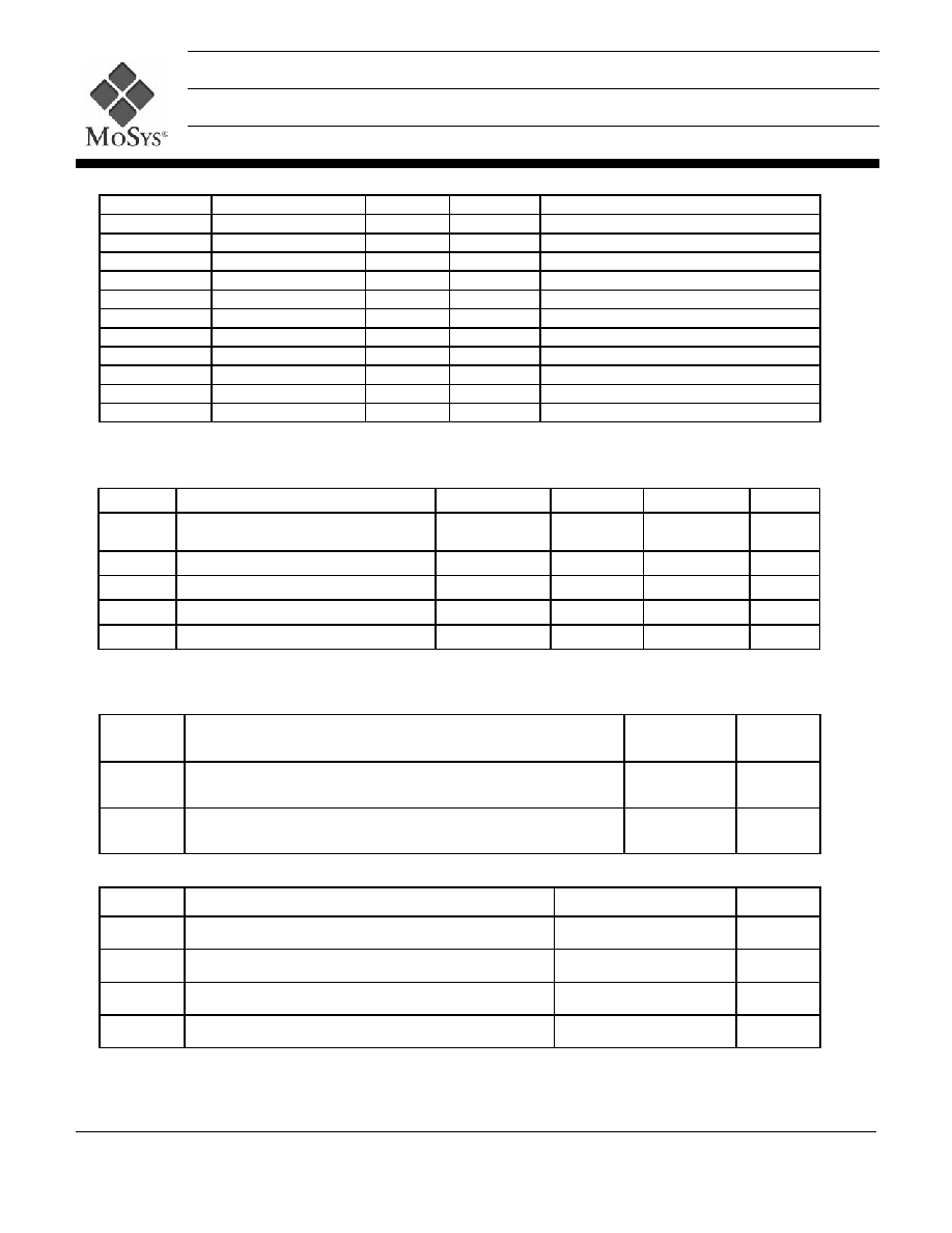
Memory Interface Signal List
Signal Name
Valid
Logic Direction
Description
adr[13:0]
Positive clk edge
Positive
Input
Memory address
rdb
Positive clk edge
Negative
Input
Memory read
wrb
Positive clk edge
Negative
Input
Memory write
din[63:0]
Positive clk edge
Positive
Input
Memory data in bus
dout[63:0]
Positive clk edge
Positive
Output
Memory data out bus
rstb
Positive clk edge
Negative
Input
Memory initialization reset
clk Clock
Positive
Input
Memory
Clock
mvddcore
Memory core supply voltage
mvsscore
Memory core ground
mvdd
Memory interface supply voltage
mvss
Memory interface ground
Recommended Operating Conditions
Symbol Parameter Condition
Min
Max
Units
VDD
Supply Voltage Range (2.5V
±
10%)
Operating 2.25
2.75 V
TJ
Junction Temperature
Nominal VDD 0
125 ∞C
tCYC Cycle
Time
Operating
6
33.3*
ns
tCKH Clock
High
Operating
0.45*tCYC 0.55*tCYC
ns
tCKL Clock
Low
Operating
0.45*tCYC 0.55*tCYC
ns
*Note: Minimum clock frequency limit adjustable to meet system timing requirements
Power Requirements
Symbol Condition Current
per Instance
Units
IDD1
Operating current, V
DD
=1.8V, clock frequency = 100MHz,
output not loaded, memory accessed every clock
0.8 mA/MHz
IDD2
Standby current, V
DD
=1.8V, clock frequency =100MHz,
memory not accessed
0.4 mA/MHz
Input Loading
Symbol
Condition
Load Capacitance
Units
CDIN
din signal input loading
0.1
pF
CADR
adr signal input loading
0.1
pF
CCTL
rdb, wrb and bweb signal input loading
0.1
pF
CCLK
clk signal input loading
1.5
pF
High Speed Pipelined 1-Mbit (16Kx64)
Standard 1T-SRAM
Æ
Embedded Memory Macro
M1T1HT25PZ64
M1T1HT25PZ64 Rev1_033
Page 3
© 2001 MoSys Inc., All Rights Reserved, 1020 Stewart Drive, Sunnyvale, CA 94085
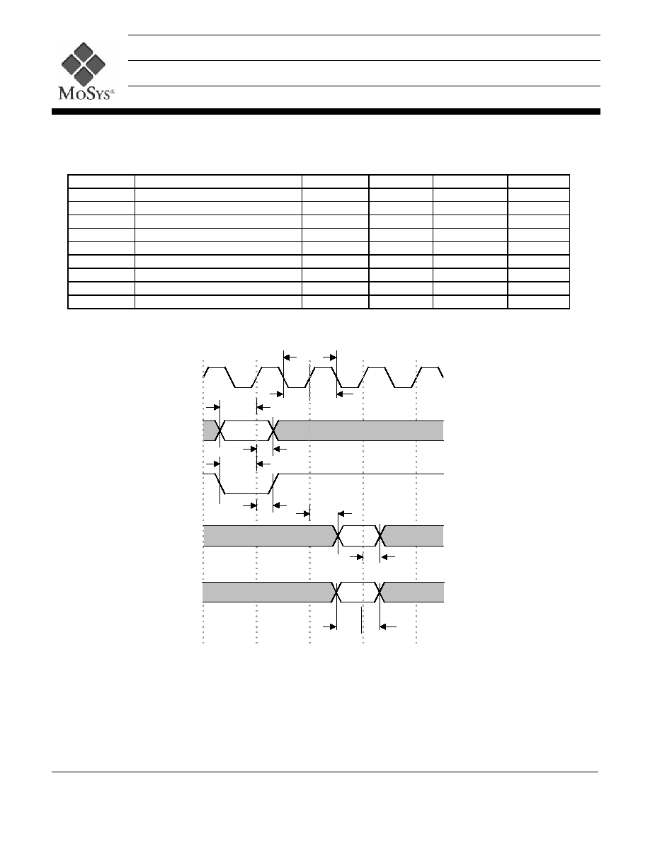
AC Timing Characteristics at Recommended Operating Conditions
All times in nanoseconds
Bolded numbers reflect worst case design parameters
Parameter
Description
Condition
Slow
Typical
Fast
tAS
Address Setup
Min.
1.5
1.2 0.9
tAH Address
Hold
Min. 0.5
0.4
0.3
tCS Control
Setup
Min. 1.5
1.2 0.9
tCH Control
Hold
Min. 0.5
0.4
0.3
tDS
Write Data Setup
Min.
1.5
1.2 0.9
tDH
Write Data Hold
Min.
0.5
0.4
0.3
tKQ
Clock to Data Valid
Max.
3.5
2.5
2.0
tKQE
Data valid extrinsic delay per pF
Max.
1.2
1.0
0.8
tKQX
Clock to Data not valid
Min.
0.8
0.6
0.4
General AC Timing
clk
adr
dout
tCYC
tCKL tCKH
A
WR/RD
rD
tKQ
tKQX
tAS
tAH
control
tCS
tCH
din
wD
tDH
tDS

High Speed Pipelined 1-Mbit (16Kx64)
Standard 1T-SRAM
Æ
Embedded Memory Macro
M1T1HT25PZ64
M1T1HT25PZ64 Rev1_033
Page 4
© 2001 MoSys Inc., All Rights Reserved, 1020 Stewart Drive, Sunnyvale, CA 94085
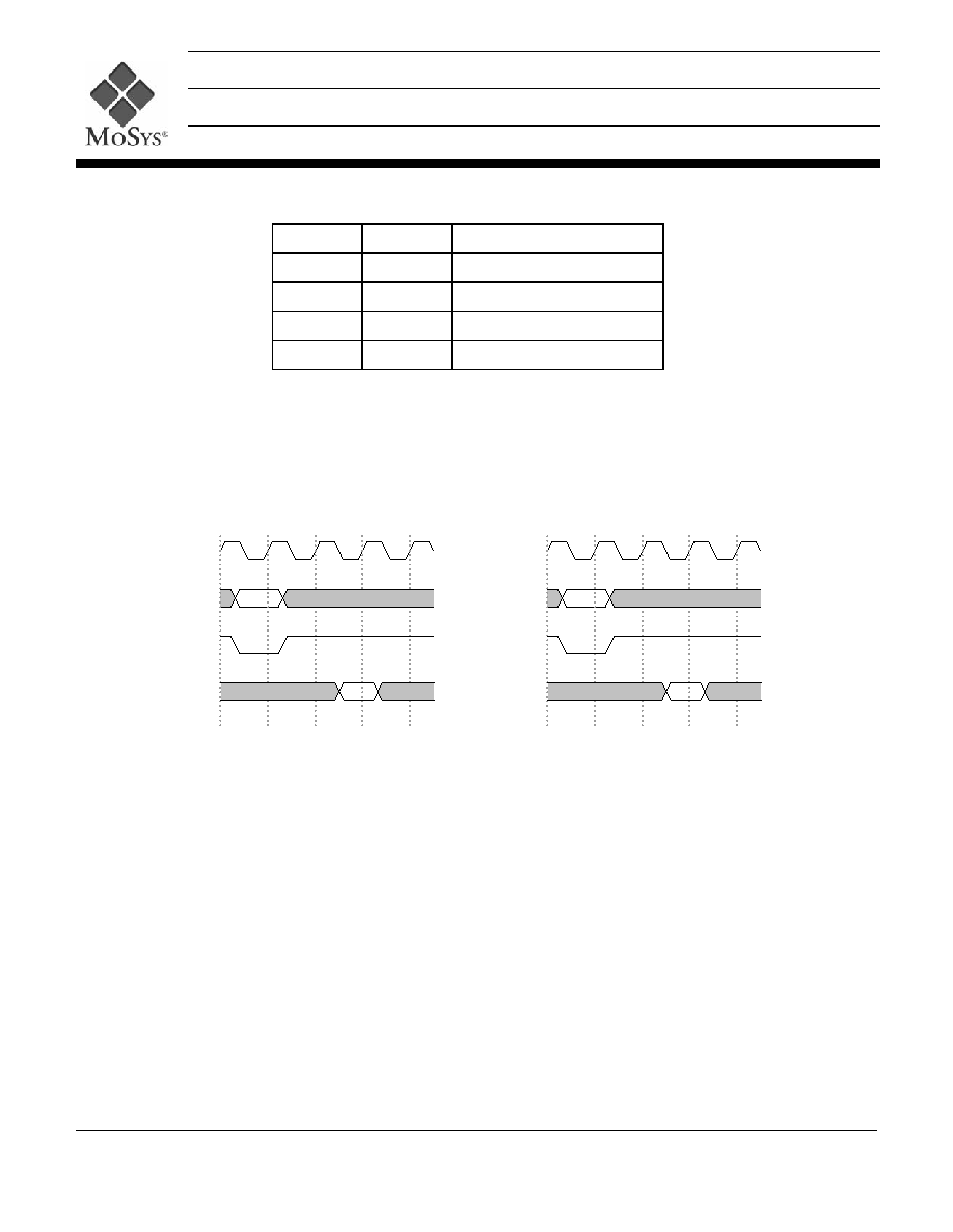
Memory macro implements a synchronous reset to force state machines into a known state after power-up.
This reset does not clear the memory contents. The clock must be running for at least two cycles before the
Reset (rstb) signal will be correctly sampled as shown above. The Reset (rstb) signal must be active for at
least ten (10) clock periods to initialize all internal circuitry. Independent of the Reset (rstb) signal, after power
has stabilized to a voltage within the operating specification and the clock is operating within its timing
specifications, there must be at least 128 clock cycles before any read or write access.
clk
rdb or wrb
rstb
>10 clk
>128 clk
Initialization Timing
High Speed Pipelined 1-Mbit (16Kx64)
Standard 1T-SRAM
Æ
Embedded Memory Macro
M1T1HT25PZ64
M1T1HT25PZ64 Rev1_033
Page 5
© 2001 MoSys Inc., All Rights Reserved, 1020 Stewart Drive, Sunnyvale, CA 94085
O
PERATION
T
RUTH
T
ABLE
rdb wrb
Operation
0 0
Illegal
0 1
Read
1 0
Write
1 1
Nop
F
UNCTIONAL
O
PERATION
Address and command clocked in by rising clock edge. Read data transfer occurs in the clock cycle following
the next clock rising edge. Write data transfer occurs in the clock cycle following the next clock rising edge.
Single Read Cycle Timing
Single Write Cycle Timing
clk
adr
dout
A
rdb
rD
clk
adr
din
A
wrb
rW