 | ÐлекÑÑоннÑй компоненÑ: 145026P | СкаÑаÑÑ:  PDF PDF  ZIP ZIP |
Äîêóìåíòàöèÿ è îïèñàíèÿ www.docs.chipfind.ru
MC145026
·
MC145027
·
MC145028
·
SC41343
·
SC41344
MOTOROLA
1
Encoder and Decoder Pairs
CMOS
These devices are designed to be used as encoder/decoder pairs in remote
control applications.
The MC145026 encodes nine lines of information and serially sends this
information upon receipt of a transmit enable (TE) signal. The nine lines may be
encoded with trinary data (low, high, or open) or binary data (low or high). The
words are transmitted twice per encoding sequence to increase security.
The MC145027 decoder receives the serial stream and interprets five of the
trinary digits as an address code. Thus, 243 addresses are possible. If binary
data is used at the encoder, 32 addresses are possible. The remaining serial
information is interpreted as four bits of binary data. The valid transmission (VT)
output goes high on the MC145027 when two conditions are met. First, two
addresses must be consecutively received (in one encoding sequence) which
both match the local address. Second, the 4 bits of data must match the last
valid data received. The active VT indicates that the information at the Data
output pins has been updated.
The MC145028 decoder treats all nine trinary digits as an address which
allows 19,683 codes. If binary data is encoded, 512 codes are possible. The VT
output goes high on the MC145028 when two addresses are consecutively
received (in one encoding sequence) which both match the local address.
·
Operating Temperature Range: 40 to + 85
°
C
·
VeryLow Standby Current for the Encoder: 300 nA Maximum @ 25
°
C
·
Interfaces with RF, Ultrasonic, or Infrared Modulators and Demodulators
·
RC Oscillator, No Crystal Required
·
High External Component Tolerance; Can Use
±
5% Components
·
Internal PowerOn Reset Forces All Decoder Outputs Low
·
Operating Voltage Range: MC145026 = 2.5 to 18 V
*
MC145027, MC145028 = 4.5 to 18 V
·
LowVoltage Versions Available:
SC41343 = 2.8 to 10 V Version of the MC145027
SC41344 = 2.8 to 10 V Version of the MC145028
·
For Infrared Applications, See Application Note AN1016/D
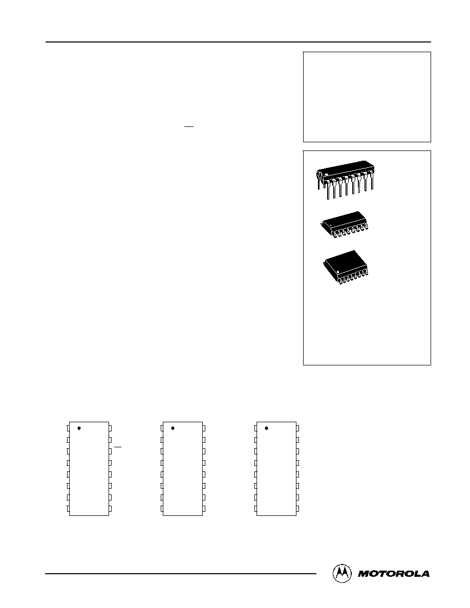
PIN ASSIGNMENTS
MC145026
ENCODER
MC145028/SC41344
DECODERS
MC145027/SC41343
DECODERS
13
14
15
16
9
10
11
12
5
4
3
2
1
8
7
6
CTC
RTC
TE
Dout
VDD
A8/D8
A9/D9
RS
A4
A3
A2
A1
VSS
A7/D7
A6/D6
A5
13
14
15
16
9
10
11
12
5
4
3
2
1
8
7
6
D9
D8
D7
D6
VDD
Din
R2/C2
VT
A4
A3
A2
A1
VSS
C1
R1
A5
13
14
15
16
9
10
11
12
5
4
3
2
1
8
7
6
A9
A8
A7
A6
VDD
Din
R2/C2
VT
A4
A3
A2
A1
VSS
C1
R1
A5
* All MC145026 devices manufactured after date code 9314 or 314 are guaranteed over this wider voltage range. All previous designs using the
lowvoltage SC41342 should convert to the MC145026, which is a dropin replacement. The SC41342 part number has been discontinued.
Order this document
by MC145026/D
MOTOROLA
SEMICONDUCTOR TECHNICAL DATA
MC145026
MC145027
MC145028
SC41343
SC41344
P SUFFIX
PLASTIC DIP
CASE 648
ORDERING INFORMATION
MC145026P
Plastic DIP
MC145026D
SOG Package
MC145027P, SC41343P
Plastic DIP
MC145027DW, SC41343DW
SOG Package
MC145028P, SC41344P
Plastic DIP
MC145028DW, SC41344DW
SOG Package
D SUFFIX
SOG PACKAGE
CASE 751B
DW SUFFIX
SOG PACKAGE
CASE 751G
16
1
16
1
16
1
©
Motorola, Inc. 1998
REV 2
1/98
MC145026
·
MC145027
·
MC145028
·
SC41343
·
SC41344
MOTOROLA
2
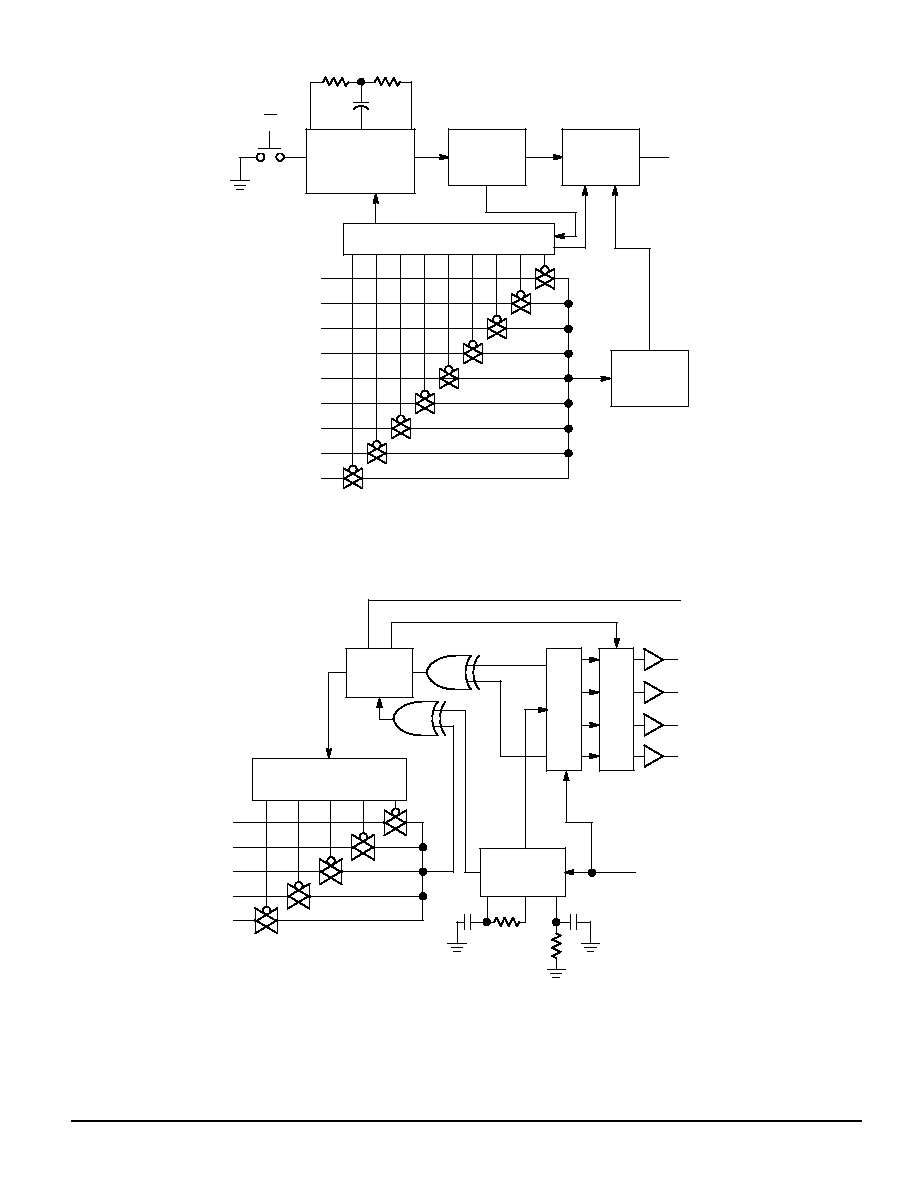
Figure 1. MC145026 Encoder Block Diagram
TE
15
RING COUNTER AND 1OF9 DECODER
9
8
7
6
5
4
3
2
1
1
2
3
4
5
6
7
9
10
RS
RTC
CTC
13
12
14
3PIN
OSCILLATOR
AND
ENABLE
÷
4
DIVIDER
DATA SELECT
AND
BUFFER
Dout
TRINARY
DETECTOR
VDD = PIN 16
VSS = PIN 8
A1
A2
A3
A4
A5
A6/D6
A7/D7
A8/D8
A9/D9
11
5
4
3
2
1
SEQUENCER CIRCUIT
1
2
3
4
5
A1
A2
A3
A4
A5
CONTROL
LOGIC
11
15
D6
LA
TCH
VT
4BIT
SHIFT
REGISTER
9
Din
DATA
EXTRACTOR
VDD = PIN 16
VSS = PIN 8
C1
C2
R2
R1
7
6
Figure 2. MC145027 Decoder Block Diagram
10
D7
D8
D9
14
13
12
MC145026
·
MC145027
·
MC145028
·
SC41343
·
SC41344
MOTOROLA
3
9
8
7
6
5
4
3
2
1
SEQUENCER CIRCUIT
1
2
3
4
5
15
14
13
12
A1
A2
A3
A4
A5
A6
A7
A8
A9
CONTROL
LOGIC
9BIT
SHIFT
REGISTER
9
Din
11
VT
DATA
EXTRACTOR
Figure 3. MC145028 Decoder Block Diagram
VDD = PIN 16
VSS = PIN 8
C1
C2
R2
R1
7
6
10
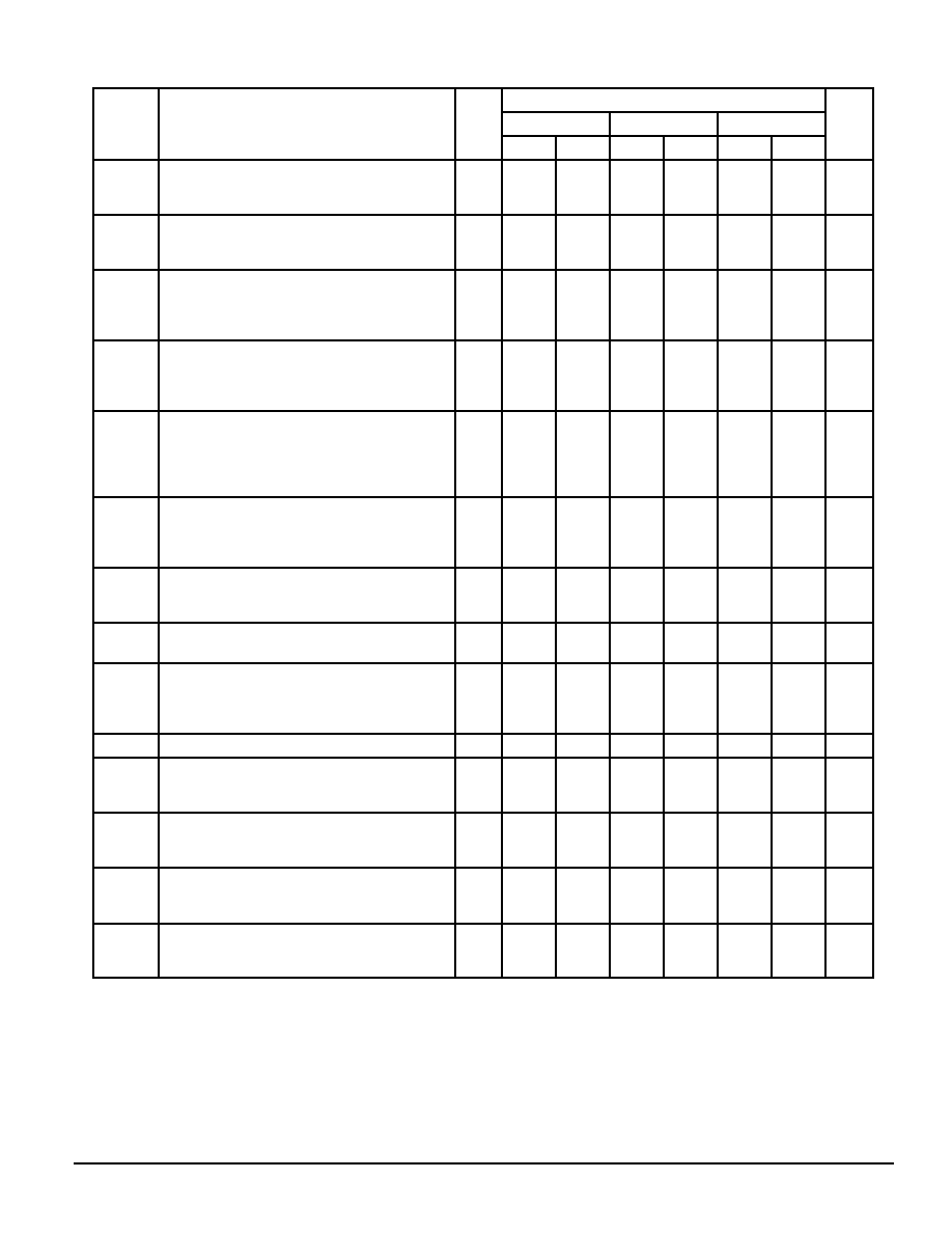
MAXIMUM RATINGS*
(Voltages Referenced to VSS)
Rating
Symbol
Value
Unit
VDD
DC Supply Voltage (except SC41343,
SC41344)
0.5 to + 18
V
VDD
DC Supply Voltage (SC41343, SC41344
only)
0.5 to + 10
V
Vin
DC Input Voltage
0.5 to VDD + 0.5
V
Vout
DC Output Voltage
0.5 to VDD + 0.5
V
Iin
DC Input Current, per Pin
±
10
mA
Iout
DC Output Current, per Pin
±
10
mA
PD
Power Dissipation, per Package
500
mW
Tstg
Storage Temperature
65 to + 150
°
C
TL
Lead Temperature, 1 mm from Case for
10 Seconds
260
°
C
* Maximum Ratings are those values beyond which damage to the device may occur. Func-
tional operation should be restricted to the limits in the Electrical Characteristics tables or
Pin Descriptions section.
This device contains protection circuitry to
guard against damage due to high static
voltages or electric fields. However, precau-
tions must be taken to avoid applications of any
voltage higher than maximum rated voltages
to this highimpedance circuit. For proper
operation, Vin and Vout should be constrained
to the range VSS
(Vin or Vout)
VDD.
MC145026
·
MC145027
·
MC145028
·
SC41343
·
SC41344
MOTOROLA
4
ELECTRICAL CHARACTERISTICS -- MC145026
*
, MC145027, and MC145028
(Voltage Referenced to VSS)
S
b l
Ch
i i
V
Guaranteed Limit
U i
S
b l
Ch
i i
VDD
40
°
C
25
°
C
85
°
C
U i
Symbol
Characteristic
VDD
V
Min
Max
Min
Max
Min
Max
Unit
VOL
LowLevel Output Voltage
(Vin = VDD or 0)
5.0
10
15
--
--
--
0.05
0.05
0.05
--
--
--
0.05
0.05
0.05
--
--
--
0.05
0.05
0.05
V
VOH
HighLevel Output Voltage
(Vin = 0 or VDD)
5.0
10
15
4.95
9.95
14.95
--
--
--
4.95
9.95
14.95
--
--
--
4.95
9.95
14.95
--
--
--
V
VIL
LowLevel Input Voltage
(Vout = 4.5 or 0.5 V)
(Vout = 9.0 or 1.0 V)
(Vout = 13.5 or 1.5 V)
5.0
10
15
--
--
--
1.5
3.0
4.0
--
--
--
1.5
3.0
4.0
--
--
--
1.5
3.0
4.0
V
VIH
HighLevel Input Voltage
(Vout = 0.5 or 4.5 V)
(Vout = 1.0 or 9.0 V)
(Vout = 1.5 or 13.5 V)
5.0
10
15
3.5
7.0
11
--
--
--
3.5
7.0
11
--
--
--
3.5
7.0
11
--
--
--
V
IOH
HighLevel Output Current
(Vout = 2.5 V)
(Vout = 4.6 V)
(Vout = 9.5 V)
(Vout = 13.5 V)
5.0
5.0
10
15
2.5
0.52
1.3
3.6
--
--
--
--
2.1
0.44
1.1
3.0
--
--
--
--
1.7
0.36
0.9
2.4
--
--
--
--
mA
IOL
LowLevel Output Current
(Vout = 0.4 V)
(Vout = 0.5 V)
(Vout = 1.5 V)
5.0
10
15
0.52
1.3
3.6
--
--
--
0.44
1.1
3.0
--
--
--
0.36
0.9
2.4
--
--
--
mA
Iin
Input Current -- TE
(MC145026, PullUp Device)
5.0
10
15
--
--
--
--
--
--
3.0
16
35
11
60
120
--
--
--
--
--
--
µ
A
Iin
Input Current
RS (MC145026), Din (MC145027, MC145028)
15
--
±
0.3
--
±
0.3
--
±
1.0
µ
A
Iin
Input Current
A1 A5, A6/D6 A9/D9 (MC145026),
A1 A5 (MC145027),
A1 A9 (MC145028)
5.0
10
15
--
--
--
--
--
--
--
--
--
±
110
±
500
±
1000
--
--
--
--
--
--
µ
A
Cin
Input Capacitance (Vin = 0)
--
--
--
--
7.5
--
--
pF
IDD
Quiescent Current -- MC145026
5.0
10
15
--
--
--
--
--
--
--
--
--
0.1
0.2
0.3
--
--
--
--
--
--
µ
A
IDD
Quiescent Current -- MC145027, MC145028
5.0
10
15
--
--
--
--
--
--
--
--
--
50
100
150
--
--
--
--
--
--
µ
A
Idd
Dynamic Supply Current -- MC145026
(fc = 20 kHz)
5.0
10
15
--
--
--
--
--
--
--
--
--
200
400
600
--
--
--
--
--
--
µ
A
Idd
Dynamic Supply Current -- MC145027, MC145028
(fc = 20 kHz)
5.0
10
15
--
--
--
--
--
--
--
--
--
400
800
1200
--
--
--
--
--
--
µ
A
* Also see next Electrical Characteristics table for 2.5 V specifications.
MC145026
·
MC145027
·
MC145028
·
SC41343
·
SC41344
MOTOROLA
5
ELECTRICAL CHARACTERISTICS -- MC145026
(Voltage Referenced to VSS)
S
b l
Ch
i i
V
Guaranteed Limit
U i
S
b l
Ch
i i
VDD
40
°
C
25
°
C
85
°
C
U i
Symbol
Characteristic
VDD
V
Min
Max
Min
Max
Min
Max
Unit
VOL
LowLevel Output Voltage
(Vin = 0 V or VDD)
2.5
--
0.05
--
0.05
--
0.05
V
VOH
HighLevel Output Voltage
(Vin = 0 V or VDD)
2.5
2.45
--
2.45
--
2.45
--
V
VIL
LowLevel Input Voltage
(Vout = 0.5 V or 2.0 V)
2.5
--
0.3
--
0.3
--
0.3
V
VIH
HighLevel Input Voltage
(Vout = 0.5 V or 2.0 V)
2.5
2.2
--
2.2
--
2.2
--
V
IOH
HighLevel Output Current
(Vout = 1.25 V)
2.5
0.28
--
0.25
--
0.2
--
mA
IOL
LowLevel Output Current
(Vout = 0.4 V)
2.5
0.22
--
0.2
--
0.16
--
mA
Iin
Input Current (TE -- PullUp Device)
2.5
--
--
0.09
1.8
--
--
µ
A
Iin
Input Current (A1A5, A6/D6A9/D9)
2.5
--
--
--
±
25
--
--
µ
A
IDD
Quiescent Current
2.5
--
--
--
0.05
--
--
µ
A
Idd
Dynamic Supply Current (fc = 20 kHz)
2.5
--
--
--
40
--
--
µ
A
ELECTRICAL CHARACTERISTICS -- SC41343 and SC41344
(Voltage Referenced to VSS)
S
b l
Ch
i i
V
Guaranteed Limit
U i
S
b l
Ch
i i
VDD
40
°
C
25
°
C
85
°
C
U i
Symbol
Characteristic
VDD
V
Min
Max
Min
Max
Min
Max
Unit
VOL
LowLevel Output Voltage
(Vin = 0 V or VDD)
2.8
5.0
10
--
--
--
0.05
0.05
0.05
--
--
--
0.05
0.05
0.05
--
--
--
0.05
0.05
0.05
V
VOH
HighLevel Output Voltage
(Vin = 0 V or VDD)
2.8
5.0
10
2.75
4.95
9.95
--
--
--
2.75
4.95
9.95
--
--
--
2.75
4.95
9.95
--
--
--
V
VIL
LowLevel Input Voltage
(Vout = 2.3 V or 0.5 V)
(Vout = 4.5 V or 0.5 V)
(Vout = 9.0 V or 1.0 V)
2.8
5.0
10
--
--
--
0.84
1.5
3.0
--
--
--
0.84
1.5
3.0
--
--
--
0.84
1.5
3.0
V
VIH
HighLevel Input Voltage
(Vout = 0.5 V or 2.3 V)
(Vout = 0.5 V or 4.5 V)
(Vout = 1.0 V or 9.0 V)
2.8
5.0
10
1.96
3.5
7.0
--
--
--
1.96
3.5
7.0
--
--
--
1.96
3.5
7.0
--
--
--
V
IOH
HighLevel Output Current
(Vout = 1.4 V)
(Vout = 4.5 V)
(Vout = 9.0 V)
2.8
5.0
10
0.73
0.59
1.3
--
--
--
0.7
0.5
1.1
--
--
--
0.55
0.41
0.9
--
--
--
mA
IOL
LowLevel Output Current
(Vout = 0.4 V)
(Vout = 0.5 V)
(Vout = 1.0 V)
2.8
5.0
10
0.35
0.8
3.5
--
--
--
0.3
0.6
2.9
--
--
--
0.24
0.4
2.3
--
--
--
mA
Iin
Input Current -- Din
10
--
±
0.3
--
±
0.3
--
±
1.0
µ
A
Iin
Input Current
A1 A5 (SC41343)
A1 A9 (SC41344)
2.8
5.0
10
--
--
--
--
--
--
--
--
--
±
30
±
140
±
600
--
--
--
--
--
--
µ
A
Cin
Input Capacitance (Vin = 0)
--
--
--
--
7.5
--
--
pF
IDD
Quiescent Current
2.8
5.0
10
--
--
--
--
--
--
--
--
--
60
75
150
--
--
--
--
--
--
µ
A
Idd
Dynamic Supply Current (fc = 20 kHz)
2.8
5.0
10
--
--
--
--
--
--
--
--
--
300
500
1000
--
--
--
--
--
--
µ
A