 | –≠–ª–µ–∫—Ç—Ä–æ–Ω–Ω—ã–π –∫–æ–º–ø–æ–Ω–µ–Ω—Ç: 1N5294 | –°–∫–∞—á–∞—Ç—å:  PDF PDF  ZIP ZIP |
MOTOROLA
SEMICONDUCTOR
TECHNICAL DATA
Motorola TVS/Zener Device Data
9-2
1.5 Watt DC Power Data Sheet
Current Regulator Diodes
Field-effect current regulator diodes are circuit elements that provide a current
essentially independent of voltage. These diodes are especially designed for maximum
impedance over the operating range. These devices may be used in parallel to obtain
higher currents.
Manufacturing Locations:
WAFER FAB: Phoenix, Arizona
ASSEMBLY/TEST: Phoenix, Arizona
MAXIMUM RATINGS
Rating
Symbol
Value
Unit
Peak Operating Voltage
(TJ = ≠55
∞
C to +200
∞
C)
POV
100
Volts
Steady State Power Dissipation
@ TL = 75
∞
C
Derate above TL = 75
∞
C
Lead Length = 3/8
(Forward or Reverse Bias)
PD
600
4.8
mW
mW/
∞
C
Operating and Storage Junction
Temperature Range
TJ, Tstg
≠55 to +200
∞
C
1N5283
through
1N5314
CURRENT
REGULATOR
DIODES
CASE 51-02
1N5283 through 1N5314
Motorola TVS/Zener Device Data
9-3
1.5 Watt DC Power Data Sheet
Devices listed in bold, italic are Motorola preferred devices.
ELECTRICAL CHARACTERISTICS
(TA = 25
∞
C unless otherwise noted)
Type No.
Regulator Current
IP (mA) @ VT = 25 V
Minimum
Dynamic
Impedance
@ VT = 25 V
ZT (M
)
Minimum
Knee
Impedance
@ VK = 6.0 V
ZK (M
)
Maximum
Limiting
Voltage
@ IL = 0.8 IP (min)
VL (Volts)
Type No.
Nom
Min
Max
Impedance
@ VT = 25 V
ZT (M
)
Impedance
@ VK = 6.0 V
ZK (M
)
Voltage
@ IL = 0.8 IP (min)
VL (Volts)
1N5283
0.22
0.198
0.242
25.0
2.75
1.00
1N5284
0.24
0.216
0.264
19.0
2.35
1.00
1N5285
0.27
0.243
0.297
14.0
1.95
1.00
1N5286
0.30
0.270
0.330
9.00
1.60
1.00
1N5287
0.33
0.297
0.363
6.60
1.35
1.00
1N5288
0.39
0.351
0.429
4.10
1.00
1.05
1N5289
0.43
0.387
0.473
3.30
0.870
1.05
1N5290
0.47
0.423
0.517
2.70
0.750
1.05
1N5291
0.56
0.504
0.616
1.90
0.560
1.10
1N5292
0.62
0.558
0.682
1.55
0.470
1.13
1N5293
0.68
0.612
0.748
1.35
0.400
1.15
1N5294
0.75
0.675
0.825
1.15
0.335
1.20
1N5295
0.82
0.738
0.902
1.00
0.290
1.25
1N5296
0.91
0.819
1.001
0.880
0.240
1.29
1N5297
1.00
0.900
1.100
0.800
0.205
1.35
1N5298
1.10
0.990
1.21
0.700
0.180
1.40
1N5299
1.20
1.08
1.32
0.640
0.155
1.45
1N5300
1.30
1.17
1.43
0.580
0.135
1.50
1N5301
1.40
1.26
1.54
0.540
0.115
1.55
1N5302
1.50
1.35
1.65
0.510
0.105
1.60
1N5303
1.60
1.44
1.76
0.475
0.092
1.65
1N5304
1.80
1.62
1.98
0.420
0.074
1.75
1N5305
2.00
1.80
2.20
0.395
0.061
1.85
1N5306
2.20
1.98
2.42
0.370
0.052
1.95
1N5307
2.40
2.16
2.64
0.345
0.044
2.00
1N5308
2.70
2.43
2.97
0.320
0.035
2.15
1N5309
3.00
2.70
3.30
0.300
0.029
2.25
1N5310
3.30
2.97
3.63
0.280
0.024
2.35
1N5311
3.60
3.24
3.96
0.265
0.020
2.50
1N5312
3.90
3.51
4.29
0.255
0.017
2.60
1N5313
4.30
3.87
4.73
0.245
0.014
2.75
1N5314
4.70
4.23
5.17
0.235
0.012
2.90
1N5283 through 1N5314
Motorola TVS/Zener Device Data
9-4
1.5 Watt DC Power Data Sheet
5
4
3
2
1
0
≠20
≠40
≠60
≠80
≠100
300
250
200
150
100
50
10
7
5
3
2
1
0.7
0.5
0.3
0.2
0.1
≠2
≠1
0
20
40
60
80
100
120
140
160
0
0.2
0.4
0.6
0.8
1
0.1
0.2
0.3
0.5
0.7
1
2
3
5
7
10
20
30
50
70
100
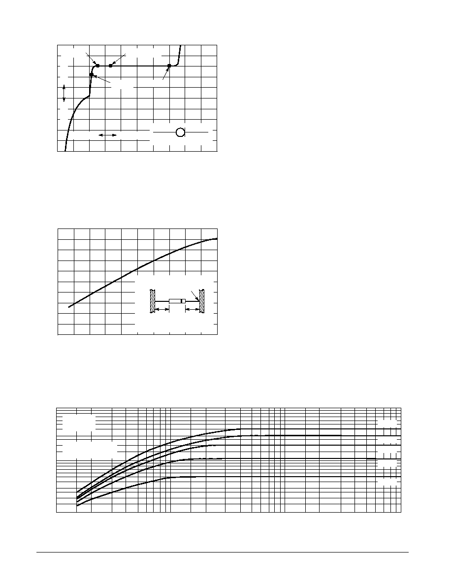
REVERSE
FORWARD
ANODE
CATHODE
+
≠
ZK @ VK
VL @ IL
POV
IP & ZT @ VT
VAK, ANODE-CATHODE VOLTAGE (VOLTS)
REVERSE
FOR
W
ARD
I D
, DIODE CURRENT
(mA)
L, LEAD LENGTH (INCHES)
JL
, JUNCTION-T
O-LEAD
THERMAL
RESIST
ANCE (
C/W)
∞
POINT OF LEAD TEMPERATURE
MEASUREMENT
(MOST HEAT CONDUCTION IS
THROUGH THE CATHODE LEAD)
L
L
1N5313
1N5309
1N5305
1N5298
1N5290
TJ = 25
∞
C
POV = 100 V
(DATA OBTAINED
FROM PULSE TESTS)
VAK, ANODE-CATHODE VOLTAGE (VOLTS)
I D
, FOR
W
ARD DIODE CURRENT
(mA)
Diode Current.
Limiting Current: 80% of IP minimum used to determine
Limiting voltage, VL.
Pinch-off Current: Regulator current at specified Test
Voltage, VT.
Peak Operating Voltage: Maximum voltage to be applied
to device.
Current Temperature Coefficient.
Anode-to-cathode Voltage.
Knee Impedance Test Voltage: Specified voltage used to
establish Knee Impedance, ZK.
Limiting Voltage: Measured at IL, VL, together with Knee
AC Impedance, ZK, indicates the Knee characteristics of
the device.
Test Voltage: Voltage at which IP and ZT are specified.
Knee AC Impedance at Test Voltage: To test for ZK, a 90
Hz signal VK with RMS value equal to 10% of test voltage,
VK, is superimposed on VK:
ZK = VK/iK
where iK is the resultant ac current due to VK.
To provide the most constant current from the diode, ZK
should be as high as possible; therefore, a minimum value
of ZK is specified.
AC Impedance at Test Voltage: Specified as a minimum
value. To test for ZT, a 90 Hz signal with RMS value equal
to 10% of Test Voltage VT, is superimposed on VT.
SYMBOLS AND DEFINITIONS
APPLICATION NOTE
As the current available from the diode is temperature dependent,
it is necessary to determine junction temperature, TJ, under specific
operating conditions to calculate the value of the diode current. The
following procedure is recommended:
Lead Temperature, TL, shall be determined from:
TL =
LA PD + TA
where
LA is lead-to-ambient thermal resistance
and
PD is power dissipation.
LA is generally 30≠40
∞
C/W for the various clips and tie points
in common use, and for printed circuit-board wiring.
Junction Temperature, TJ, shall be calculated from:
TJ = TL +
JL PD
where
JL is taken from Figure 2.
For circuit design limits of VAK, limits of PD may be estimated and
extremes of TJ may be computed. Using the information on Figures
4 and 5, changes in current may be found. To improve current
regulation, keep VAK low to reduce PD and keep the leads short,
especially the cathode lead, to reduce
JL.
Figure 1. Typical Current Regulator
Characteristics
Figure 2. Typical Thermal Resistance
Figure 3. Typical Forward Characteristics
ID --
IL --
IP --
POV --
l --
VAK --
VK --
VL --
VT --
ZK --
ZT --
1N5283 through 1N5314
Motorola TVS/Zener Device Data
9-5
1.5 Watt DC Power Data Sheet
Devices listed in bold, italic are Motorola preferred devices.
0.7
0.6
0.5
0.4
0.3
0.2
0.1
0
≠0.1
≠0.2
≠0.3
≠0.4
≠0.5
1
0.8
0.6
0.4
0.2
0
≠0.2
≠0.4
≠0.6
≠0.8
≠1
0.1
0
≠0.1
≠0.2
≠0.3
≠0.4
≠0.5
≠0.6
≠0.7
≠0.8
≠0.9
≠1
≠1.1
0.2
0.3
0.4
0.5
0.6
0.7
0.8
0.9
1
2
3
4
5
0.2
0.3
0.4
0.5
0.6
0.7
0.8
0.9
1
2
3
4
5
0.2
0.3
0.4
0.5
0.6
0.7
0.8
0.9
1
2
3
4
5
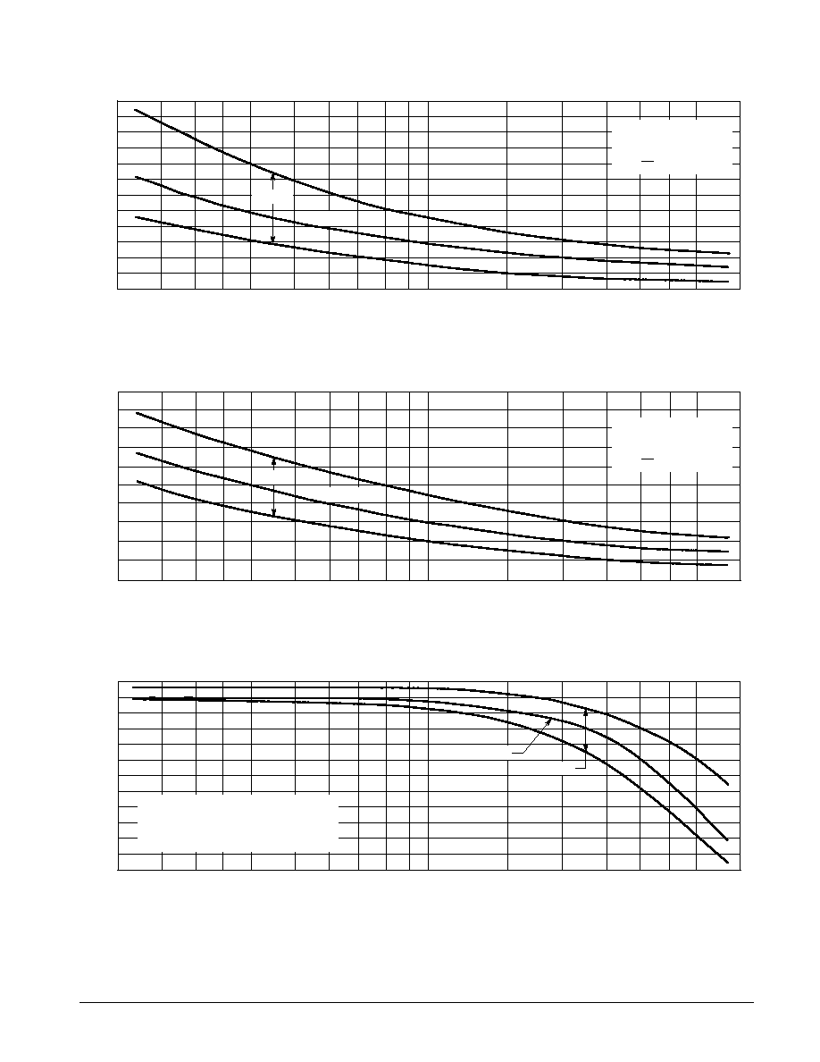
TYPICAL
RANGE*
TYPICAL
RANGE*
RANGE*
TYPICAL
IP, NOMINAL PINCH-OFF CURRENT (mA)
IP, NOMINAL PINCH-OFF CURRENT (mA)
IP, NOMINAL PINCH-OFF CURRENT (mA)
I,
TEMPERA
TURE COEFFICIENT
(%/
C)
∞
I,
TEMPERA
TURE COEFFICIENT
(%/
C)
∞
I P
, CURRENT
CHANGE (mA)
TJ = +25
∞
C TO +150
∞
C
VAK = 25 V
IP =
I
100
IP(nom)
TJ (
∞
C)
TJ = ≠55
∞
C TO +25
∞
C
VAK = 25 V
IP =
I
100
IP(nom)
TJ (
∞
C)
TA = 25
∞
C
VAK = 40 V, VAK VARIED FROM 10 V TO 50 V
IP = IP @ 50 V ≠ IP @ 10 V
1/2
LEAD LENGTH,
LA = 30
∞
C/W
*90% of the units will be in the ranges shown.
Figure 4. Temperature Coefficient
Figure 5. Temperature Coefficient
Figure 6. Current Regulation Factor
1N5283 through 1N5314
Motorola TVS/Zener Device Data
9-6
1.5 Watt DC Power Data Sheet
1.5 Watt DC Power
MULTIPLE PACKAGE QUANTITY (MPQ)
REQUIREMENTS
Current Regulator Diodes -- Axial Leaded
CASE 51-02
DO-204AA
GLASS
(Refer to Section 10 for Surface Mount, Thermal Data and Footprint Information.)
(Refer to Section 10 for more information on Packaging Specifications.)
Package Option
Tape and Reel
2.5K
Type No. Suffix
RL
MPQ (Units)
Bulk
(None)
500
NOTES:
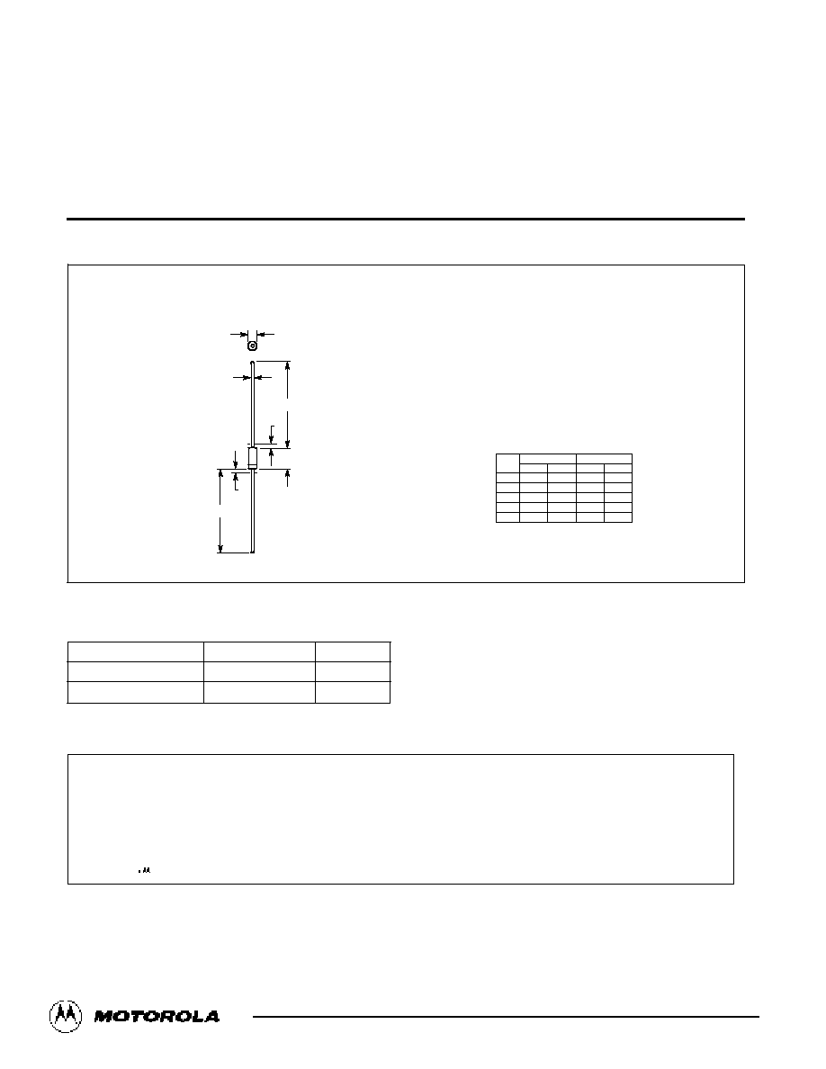
1. PACKAGE CONTOUR OPTIONAL WITHIN DIA B
AND LENGTH A. HEAT SLUGS, IF ANY, SHALL BE
INCLUDED WITHIN THIS CYLINDER, BUT SHALL
NOT BE SUBJECT TO THE MIN LIMIT OF DIA B.
2. LEAD DIA NOT CONTROLLED IN ZONES F, TO
ALLOW FOR FLASH, LEAD FINISH BUILDUP,
AND MINOR IRREGULARITIES OTHER THAN
HEAT SLUGS.
A
K
D
F
B
K
F
MIN
MIN
MAX
MAX
MILLIMETERS
INCHES
DIM
5.84
2.16
0.46
--
25.40
7.62
2.72
0.56
1.27
38.10
0.230
0.085
0.018
--
1.000
0.300
0.107
0.022
0.050
1.500
A
B
D
F
K
All JEDEC dimensions and notes apply
Motorola reserves the right to make changes without further notice to any products herein. Motorola makes no warranty, representation or guarantee regarding
the suitability of its products for any particular purpose, nor does Motorola assume any liability arising out of the application or use of any product or circuit,
and specifically disclaims any and all liability, including without limitation consequential or incidental damages. "Typical" parameters can and do vary in different
applications. All operating parameters, including "Typicals" must be validated for each customer application by customer's technical experts. Motorola does
not convey any license under its patent rights nor the rights of others. Motorola products are not designed, intended, or authorized for use as components in
systems intended for surgical implant into the body, or other applications intended to support or sustain life, or for any other application in which the failure of
the Motorola product could create a situation where personal injury or death may occur. Should Buyer purchase or use Motorola products for any such
unintended or unauthorized application, Buyer shall indemnify and hold Motorola and its officers, employees, subsidiaries, affiliates, and distributors harmless
against all claims, costs, damages, and expenses, and reasonable attorney fees arising out of, directly or indirectly, any claim of personal injury or death
associated with such unintended or unauthorized use, even if such claim alleges that Motorola was negligent regarding the design or manufacture of the part.
Motorola and
are registered trademarks of Motorola, Inc. Motorola, Inc. is an Equal Opportunity/Affirmative Action Employer.
Literature Distribution Centers:
USA: Motorola Literature Distribution; P.O. Box 20912; Phoenix, Arizona 85036.
EUROPE: Motorola Ltd.; European Literature Centre; 88 Tanners Drive, Blakelands, Milton Keynes, MK14 5BP, England.
JAPAN: Nippon Motorola Ltd.; 4-32-1, Nishi-Gotanda, Shinagawa-ku, Tokyo 141, Japan.
ASIA PACIFIC: Motorola Semiconductors H.K. Ltd.; Silicon Harbour Center, No. 2 Dai King Street, Tai Po Industrial Estate, Tai Po, N.T., Hong Kong.