 | ÐлекÑÑоннÑй компоненÑ: 1N5913B | СкаÑаÑÑ:  PDF PDF  ZIP ZIP |
Äîêóìåíòàöèÿ è îïèñàíèÿ www.docs.chipfind.ru
MOTOROLA
SEMICONDUCTOR
TECHNICAL DATA
Motorola TVS/Zener Device Data
6-43
13 Watt DO-41 Surmetic 30 Data Sheet
1 to 3 Watt DO-41 Surmetic 30
Zener Voltage Regulator Diodes
GENERAL DATA APPLICABLE TO ALL SERIES IN
THIS GROUP
1 to 3 Watt Surmetic 30
Silicon Zener Diodes
. . . a complete series of 1 to 3 Watt Zener Diodes with limits and operating characteristics
that reflect the superior capabilities of silicon-oxide-passivated junctions. All this in an
axial-lead, transfer-molded plastic package offering protection in all common environmen-
tal conditions.
Specification Features:
·
Surge Rating of 98 Watts @ 1 ms
·
Maximum Limits Guaranteed On Up To Six Electrical Parameters
·
Package No Larger Than the Conventional 1 Watt Package
Mechanical Characteristics:
CASE: Void-free, transfer-molded, thermosetting plastic
FINISH: All external surfaces are corrosion resistant and leads are readily solderable
POLARITY: Cathode indicated by color band. When operated in zener mode, cathode
will be positive with respect to anode
MOUNTING POSITION: Any
WEIGHT: 0.4 gram (approx)
WAFER FAB LOCATION: Phoenix, Arizona
ASSEMBLY/TEST LOCATION: Seoul, Korea
MAXIMUM RATINGS
Rating
Symbol
Value
Unit
DC Power Dissipation @ TL = 75
°
C
Lead Length = 3/8
Derate above 75
°
C
PD
3
24
Watts
mW/
°
C
DC Power Dissipation @ TA = 50
°
C
Derate above 50
°
C
PD
1
6.67
Watt
mW/
°
C
Operating and Storage Junction Temperature Range
TJ, Tstg
65 to +200
°
C
GENERAL
DATA
CASE 59-03
DO-41
PLASTIC
13 WATT
DO-41
SURMETIC 30
1 TO 3 WATT
ZENER REGULATOR
DIODES
3.3400 VOLTS
Figure 1. Power Temperature Derating Curve
TL, LEAD TEMPERATURE (
°
C)
P
, MAXIMUM DISSIP
A
TION (W
A
TTS)
D
0
20
40
60
200
80
100
120
140
160
180
0
1
2
3
4
5
L = 1/8
L = 3/8
L = 1
L = LEAD LENGTH
TO HEAT SINK
GENERAL DATA -- 1-3 WATT DO-41 SURMETIC 30
Motorola TVS/Zener Device Data
6-44
13 Watt DO-41 Surmetic 30 Data Sheet
t, TIME (SECONDS)
0.0001 0.0002
0.0005
0.001
0.002
0.005
0.01
0.02
0.05
0.1
0.2
0.5
1
2
5
10
0.3
0.5
0.7
1
2
3
5
7
10
20
30
D =0.5
0.2
0.1
0.05
0.01
D = 0
DUTY CYCLE, D =t1/t2
JL
(t, D)
TRANSIENT
THERMAL
RESIST
ANCE
JUNCTION-T
O-LEAD ( C/W)
°
PPK
t1
NOTE: BELOW 0.1 SECOND, THERMAL
RESPONSE CURVE IS APPLICABLE
TO ANY LEAD LENGTH (L).
SINGLE PULSE
TJL =
JL (t)PPK
REPETITIVE PULSES
TJL =
JL (t,D)PPK
t2
0.02
10
20
30
50
100
200
300
500
1K
0.1
0.2 0.3 0.5
1
2
3
5
10
20 30 50
100
PW, PULSE WIDTH (ms)
P
, PEAK SURGE POWER (W
A
TTS)
PK
1
2
5
10
20
50
100
200
400
1000
0.0003
0.0005
0.001
0.002
0.005
0.01
0.02
0.05
0.1
0.2
0.5
1
2
3
TA = 125
°
C
TA = 125
°
C
NOMINAL VZ (VOLTS)
AS SPECIFIED IN ELEC. CHAR.
T
ABLE
Figure 2. Typical Thermal Response L, Lead Length = 3/8 Inch
Figure 3. Maximum Surge Power
Figure 4. Typical Reverse Leakage
I R
, REVERSE LEAKAGE (
µ
Adc) @ V
R
RECTANGULAR
NONREPETITIVE
WAVEFORM
TJ = 25
°
C PRIOR
TO INITIAL PULSE
APPLICATION NOTE
Since the actual voltage available from a given zener diode
is temperature dependent, it is necessary to determine junc-
tion temperature under any set of operating conditions in order
to calculate its value. The following procedure is recom-
mended:
Lead Temperature, TL, should be determined from:
TL =
LA PD + TA
LA is the lead-to-ambient thermal resistance (
°
C/W) and
PD is the power dissipation. The value for
LA will vary and
depends on the device mounting method.
LA is generally
3040
°
C/W for the various clips and tie points in common
use and for printed circuit board wiring.
The temperature of the lead can also be measured using a
thermocouple placed on the lead as close as possible to the tie
point. The thermal mass connected to the tie point is normally
large enough so that it will not significantly respond to heat
surges generated in the diode as a result of pulsed operation
once steady-state conditions are achieved. Using the mea-
sured value of TL, the junction temperature may be deter-
mined by:
TJ = TL +
TJL
TJL is the increase in junction temperature above the lead
temperature and may be found from Figure 2 for a train of
power pulses (L = 3/8 inch) or from Figure 10 for dc power.
TJL =
JL PD
For worst-case design, using expected limits of IZ, limits of
PD and the extremes of TJ (
TJ) may be estimated. Changes
in voltage, VZ, can then be found from:
V =
VZ
TJ
VZ, the zener voltage temperature coefficient, is found from
Figures 5 and 6.
Under high power-pulse operation, the zener voltage will
vary with time and may also be affected significantly by the
zener resistance. For best regulation, keep current excursions
as low as possible.
Data of Figure 2 should not be used to compute surge capa-
bility. Surge limitations are given in Figure 3. They are lower
than would be expected by considering only junction tempera-
ture, as current crowding effects cause temperatures to be ex-
tremely high in small spots resulting in device degradation
should the limits of Figure 3 be exceeded.
GENERAL DATA -- 1-3 WATT DO-41 SURMETIC 30
Motorola TVS/Zener Device Data
6-45
13 Watt DO-41 Surmetic 30 Data Sheet
Figure 5. Units To 12 Volts
Figure 6. Units 10 To 400 Volts
Figure 7. VZ = 3.3 thru 10 Volts
Figure 8. VZ = 12 thru 82 Volts
Figure 9. VZ = 100 thru 400 Volts
Figure 10. Typical Thermal Resistance
ZENER VOLTAGE versus ZENER CURRENT
(Figures 7, 8 and 9)
TEMPERATURE COEFFICIENT RANGES
(90% of the Units are in the Ranges Indicated)
VZ, ZENER VOLTAGE @ IZT (VOLTS)
3
4
5
6
7
8
9
10
11
12
10
8
6
4
2
0
2
4
RANGE
,
TEMPERA
TURE COEFFICIENT
(mV/ C) @ I
ZT
VZ
°
1000
500
200
100
50
20
10
10
20
50
100
200
400
1000
VZ, ZENER VOLTAGE @ IZT (VOLTS)
,
TEMPERA
TURE COEFFICIENT
(mV/ C) @ I
ZT
VZ
°
0
1
2
3
4
5
6
7
8
9
10
100
50
30
20
10
1
0.5
0.3
0.2
0.1
VZ, ZENER VOLTAGE (VOLTS)
I , ZENER CURRENT
(mA)
Z
2
5
3
0
10
20
30
40
50
60
70
80
90
100
VZ, ZENER VOLTAGE (VOLTS)
I , ZENER CURRENT
(mA)
Z
100
50
30
20
10
1
0.5
0.3
0.2
0.1
2
5
3
100
200
300
400
250
350
150
10
1
0.5
0.2
0.1
VZ, ZENER VOLTAGE (VOLTS)
2
5
I , ZENER CURRENT
(mA)
Z
0
10
20
30
40
50
60
70
80
L, LEAD LENGTH TO HEAT SINK (INCH)
PRIMARY PATH OF
CONDUCTION IS THROUGH
THE CATHODE LEAD
0
1/8
1/4
3/8
1/2
5/8
3/4
7/8
1
TL
JL
, JUNCTION-T
O-LEAD
THERMAL
RESIST
ANCE
L
L
( C/W)
°
GENERAL DATA -- 1-3 WATT DO-41 SURMETIC 30
Motorola TVS/Zener Device Data
6-46
13 Watt DO-41 Surmetic 30 Data Sheet
*MAXIMUM RATINGS
Rating
Symbol
Value
Unit
DC Power Dissipation @ TL = 75
°
C, Lead Length = 3/8
Derate above 75
°
C
PD
1.5
12
Watts
mW/
°
C
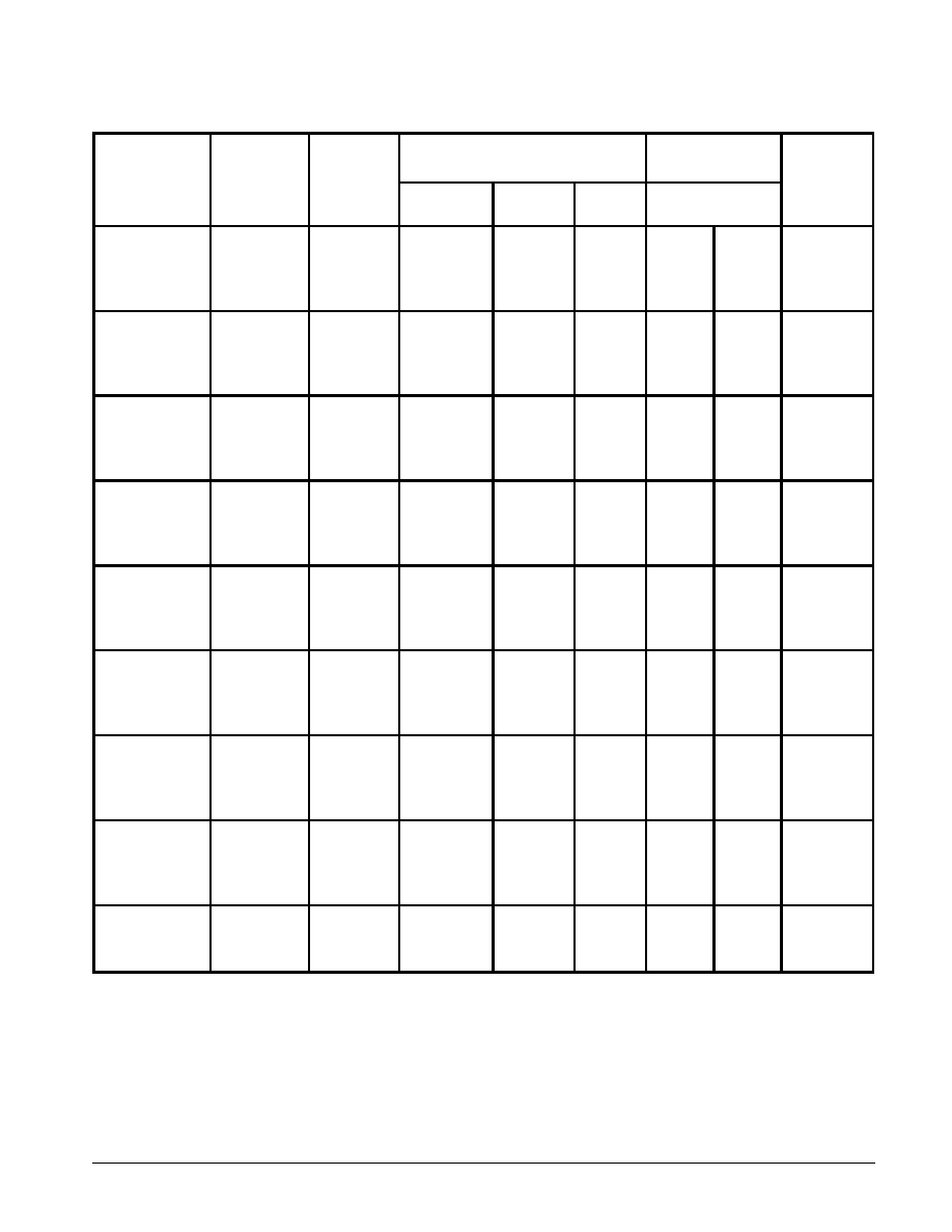
*ELECTRICAL CHARACTERISTICS
(TL = 30
°
C unless otherwise noted. VF = 1.5 Volts Max @ lF = 200 mAdc for all types.)
Motorola
Type
Number
(Note 1)
Nominal
Zener Voltage
VZ @ IZT
Volts
(Note 2 and 3)
Test
Current
IZT
mA
Max. Zener Impedance (Note 4)
Max. Reverse
Leakage Current
Maximum DC
Zener
Current
IZM
mAdc
Type
Number
(Note 1)
VZ @ IZT
Volts
(Note 2 and 3)
Current
IZT
mA
ZZT @ IZT
Ohms
ZZK
Ohms
IZK
mA
@
IR
µ
A
VR
Volts
@
Current
IZM
mAdc
1N5913B
3.3
113.6
10
500
1
100
1
454
1N5914B
3.6
104.2
9
500
1
75
1
416
1N5915B
3.9
96.1
7.5
500
1
25
1
384
1N5916B
4.3
87.2
6
500
1
5
1
348
1N5917B
4.7
79.8
5
500
1
5
1.5
319
1N5918B
5.1
73.5
4
350
1
5
2
294
1N5919B
5.6
66.9
2
250
1
5
3
267
1N5920B
6.2
60.5
2
200
1
5
4
241
1N5921B
6.8
55.1
2.5
200
1
5
5.2
220
1N5922B
7.5
50
3
400
0.5
5
6
200
1N5923B
8.2
45.7
3.5
400
0.5
5
6.5
182
1N5924B
9.1
41.2
4
500
0.5
5
7
164
1N5925B
10
37.5
4.5
500
0.25
5
8
150
1N5926B
11
34.1
5.5
550
0.25
1
8.4
136
1N5927B
12
31.2
6.5
550
0.25
1
9.1
125
1N5928B
13
28.8
7
550
0.25
1
9.9
115
1N5929B
15
25
9
600
0.25
1
11.4
100
1N5930B
16
23.4
10
600
0.25
1
12.2
93
1N5931B
18
20.8
12
650
0.25
1
13.7
83
1N5932B
20
18.7
14
650
0.25
1
15.2
75
1N5933B
22
17
17.5
650
0.25
1
16.7
68
1N5934B
24
15.6
19
700
0.25
1
18.2
62
1N5935B
27
13.9
23
700
0.25
1
20.6
55
1N5936B
30
12.5
26
750
0.25
1
22.8
50
1N5937B
33
11.4
33
800
0.25
1
25.1
45
1N5938B
36
10.4
38
850
0.25
1
27.4
41
1N5939B
39
9.6
45
900
0.25
1
29.7
38
1N5940B
43
8.7
53
950
0.25
1
32.7
34
1N5941B
47
8
67
1000
0.25
1
35.8
31
1N5942B
51
7.3
70
1100
0.25
1
38.8
29
1N5943B
56
6.7
86
1300
0.25
1
42.6
26
1N5944B
62
6
100
1500
0.25
1
47.1
24
1N5945B
68
5.5
120
1700
0.25
1
51.7
22
1N5946B
75
5
140
2000
0.25
1
56
20
1N5947B
82
4.6
160
2500
0.25
1
62.2
18
(continued)
*Indicates JEDEC Registered Data.
GENERAL DATA -- 1-3 WATT DO-41 SURMETIC 30
Motorola TVS/Zener Device Data
6-47
13 Watt DO-41 Surmetic 30 Data Sheet
*ELECTRICAL CHARACTERISTICS -- continued
(TL = 30
°
C unless otherwise noted. VF = 1.5 Volts Max @ lF = 200 mAdc for all
types.)
Motorola
Type
Number
(Note 1)
Nominal
Zener Voltage
VZ @ IZT
Volts
(Note 2 and 3)
Test
Current
IZT
mA
Max. Zener Impedance (Note 4)
Max. Reverse
Leakage Current
Maximum DC
Zener
Current
IZM
mAdc
Type
Number
(Note 1)
VZ @ IZT
Volts
(Note 2 and 3)
Current
IZT
mA
ZZT @ IZT
Ohms
ZZK
Ohms
IZK
mA
@
IR
µ
A
VR
Volts
@
Current
IZM
mAdc
1N5948B
91
4.1
200
3000
0.25
1
69.2
16
1N5949B
100
3.7
250
3100
0.25
1
76
15
1N5950B
110
3.4
300
4000
0.25
1
83.6
13
1N5951B
120
3.1
380
4500
0.25
1
91.2
12
1N5952B
130
2.9
450
5000
0.25
1
98.8
11
1N5953B
150
2.5
600
6000
0.25
1
114
10
1N5954B
160
2.3
700
6500
0.25
1
121.6
9
1N5955B
180
2.1
900
7000
0.25
1
136.8
8
1N5956B
200
1.9
1200
8000
0.25
1
152
7
*Indicates JEDEC Registered Data.
NOTE 1. TOLERANCE AND VOLTAGE DESIGNATION
Tolerance designation -- Device tolerances of
±
5% are indicated by a "B" suffix.
NOTE 2. SPECIAL SELECTIONS AVAILABLE INCLUDE:
Nominal zener voltages between those shown and
±
1% and
±
2% tight voltage tolerances.
Consult factory.
GENERAL DATA -- 1-3 WATT DO-41 SURMETIC 30
Motorola TVS/Zener Device Data
6-48
13 Watt DO-41 Surmetic 30 Data Sheet
ELECTRICAL CHARACTERISTICS
(TA = 25
°
C unless otherwise noted) VF = 1.5 V Max, IF = 200 mA for all types)
Motorola
Type No.
(Note 1)
Nominal
Zener Voltage
VZ @ IZT
Volts
(Note 2)
Test
Current
IZT
mA
Max Zener Impedance
(Note 3)
Leakage
Current
Maximum
Zener
Current
IZM
mA
Surge
Current
@ TA = 25
°
C
ir mA
(Note 4)
Motorola
Type No.
(Note 1)
VZ @ IZT
Volts
(Note 2)
Current
IZT
mA
ZZT @ IZT
Ohms
ZZK @ IZK
Ohms
IZK
mA
IR
µ
A Max
VR
Volts
@
Current
IZM
mA
@ TA = 25
°
C
ir mA
(Note 4)
3EZ3.9D5
3.9
192
4.5
400
1
80
1
630
4.4
3EZ4.3D5
4.3
174
4.5
400
1
30
1
590
4.1
3EZ4.7D5
4.7
160
4
500
1
20
1
550
3.8
3EZ5.1D5
5.1
147
3.5
550
1
5
1
520
3.5
3EZ5.6D5
5.6
134
2.5
600
1
5
2
480
3.3
3EZ6.2D5
6.2
121
1.5
700
1
5
3
435
3.1
3EZ6.8D5
6.8
110
2
700
1
5
4
393
2.9
3EZ7.5D5
7.5
100
2
700
0.5
5
5
360
2.66
3EZ8.2D5
8.2
91
2.3
700
0.5
5
6
330
2.44
3EZ9.1D5
9.1
82
2.5
700
0.5
3
7
297
2.2
3EZ10D5
10
75
3.5
700
0.25
3
7.6
270
2
3EZ11D5
11
68
4
700
0.25
1
8.4
245
1.82
3EZ12D5
12
63
4.5
700
0.25
1
9.1
225
1.66
3EZ13D5
13
58
4.5
700
0.25
0.5
9.9
208
1.54
3EZ14D5
14
53
5
700
0.25
0.5
10.6
193
1.43
3EZ15D5
15
50
5.5
700
0.25
0.5
11.4
180
1.33
3EZ16D5
16
47
5.5
700
0.25
0.5
12.2
169
1.25
3EZ17D5
17
44
6
750
0.25
0.5
13
159
1.18
3EZ18D5
18
42
6
750
0.25
0.5
13.7
150
1.11
3EZ19D5
19
40
7
750
0.25
0.5
14.4
142
1.05
3EZ20D5
20
37
7
750
0.25
0.5
15.2
135
1
3EZ22D5
22
34
8
750
0.25
0.5
16.7
123
0.91
3EZ24D5
24
31
9
750
0.25
0.5
18.2
112
0.83
3EZ27D5
27
28
10
750
0.25
0.5
20.6
100
0.74
3EZ28D5
28
27
12
750
0.25
0.5
21
96
0.71
3EZ30D5
30
25
16
1000
0.25
0.5
22.5
90
0.67
3EZ33D5
33
23
20
1000
0.25
0.5
25.1
82
0.61
3EZ36D5
36
21
22
1000
0.25
0.5
27.4
75
0.56
3EZ39D5
39
19
28
1000
0.25
0.5
29.7
69
0.51
3EZ43D5
43
17
33
1500
0.25
0.5
32.7
63
0.45
3EZ47D5
47
16
38
1500
0.25
0.5
35.6
57
0.42
3EZ51D5
51
15
45
1500
0.25
0.5
38.8
53
0.39
3EZ56D5
56
13
50
2000
0.25
0.5
42.6
48
0.36
3EZ62D5
62
12
55
2000
0.25
0.5
47.1
44
0.32
3EZ68D5
68
11
70
2000
0.25
0.5
51.7
40
0.29
3EZ75D5
75
10
85
2000
0.25
0.5
56
36
0.27
3EZ82D5
82
9.1
95
3000
0.25
0.5
62.2
33
0.24
3EZ91D5
91
8.2
115
3000
0.25
0.5
69.2
30
0.22
3EZ100D5
100
7.5
160
3000
0.25
0.5
76
27
0.2
3EZ110D5
110
6.8
225
4000
0.25
0.5
83.6
25
0.18
3EZ120D5
120
6.3
300
4500
0.25
0.5
91.2
22
0.16
3EZ130D5
130
5.8
375
5000
0.25
0.5
98.8
21
0.15
3EZ140D5
140
5.3
475
5000
0.25
0.5
106.4
19
0.14
3EZ150D5
150
5
550
6000
0.25
0.5
114
18
0.13
3EZ160D5
160
4.7
625
6500
0.25
0.5
121.6
17
0.12
3EZ170D5
170
4.4
650
7000
0.25
0.5
130.4
16
0.12
3EZ180D5
180
4.2
700
7000
0.25
0.5
136.8
15
0.11
3EZ190D5
190
4
800
8000
0.25
0.5
144.8
14
0.1
(continued)
GENERAL DATA -- 1-3 WATT DO-41 SURMETIC 30
Motorola TVS/Zener Device Data
6-49
13 Watt DO-41 Surmetic 30 Data Sheet
ELECTRICAL CHARACTERISTICS -- continued
(TA = 25
°
C unless otherwise noted) VF = 1.5 V Max, IF = 200 mA for all types)
Motorola
Type No.
(Note 1)
Nominal
Zener Voltage
VZ @ IZT
Volts
(Note 2)
Test
Current
IZT
mA
Max Zener Impedance
(Note 3)
Leakage
Current
Maximum
Zener
Current
IZM
mA
Surge
Current
@ TA = 25
°
C
ir mA
(Note 4)
Motorola
Type No.
(Note 1)
VZ @ IZT
Volts
(Note 2)
Current
IZT
mA
ZZT @ IZT
Ohms
ZZK @ IZK
Ohms
IZK
mA
IR
µ
A Max
VR
Volts
@
Current
IZM
mA
@ TA = 25
°
C
ir mA
(Note 4)
3EZ200D5
200
3.7
875
8000
0.25
0.5
152
13
0.1
3EZ220D5
220
3.4
1600
9000
0.25
1
167
12
0.09
3EZ240D5
240
3.1
1700
9000
0.25
1
182
11
0.09
3EZ270D5
270
2.8
1800
9000
0.25
1
205
10
0.08
3EZ300D5
300
2.5
1900
9000
0.25
1
228
9
0.07
3EZ330D5
330
2.3
2200
9000
0.25
1
251
8
0.06
3EZ360D5
360
2.1
2700
9000
0.25
1
274
8
0.06
3EZ400D5
400
1.9
3500
9000
0.25
1
304
7
0.06
NOTE 1. TOLERANCES
Suffix 5 indicates 5% tolerance. Any other tolerance will be considered as a special device.
NOTE 2. ZENER VOLTAGE (VZ) MEASUREMENT
Motorola guarantees the zener voltage when measured at 40 ms
±
10 ms 3/8
from the diode
body, and an ambient temperature of 25
°
C (+8
°
C, 2
°
C)
NOTE 3. ZENER IMPEDANCE (ZZ) DERIVATION
The zener impedance is derived from the 60 cycle ac voltage, which results when an ac cur-
rent having an rms value equal to 10% of the dc zener current (IZT or IZK) is superimposed
on IZT or IZK.
NOTE 4. SURGE CURRENT (ir) NON-REPETITIVE
The rating listed in the electrical characteristics table is maximum peak, non-repetitive, re-
verse surge current of 1/2 square wave or equivalent sine wave pulse of 1/120 second dura-
tion superimposed on the test current, IZT, per JEDEC standards, however, actual device ca-
pability is as described in Figure 3 of General Data sheet for Surmetic 30s.
NOTE 5. SPECIAL SELECTIONS AVAILABLE INCLUDE:
Nominal zener voltages between those shown. Tight voltage tolerances such as
±
1% and
±
2%. Consult factory.
NOTE 3. ZENER VOLTAGE (VZ) MEASUREMENT
Motorola guarantees the zener voltage when meausred at 90 seconds while maintaining the
lead temperature (TL) at 30
°
C
±
1
°
C, 3/8
from the diode body.
NOTE 4. ZENER IMPEDANCE (ZZ) DERIVATION
The zener impedance is derived from the 60 cycle ac voltage, which results when an ac cur-
rent having an rms value equal to 10% of the dc zener current (IZT or IZK) is superimposed
on IZT or IZK.
GENERAL DATA -- 1-3 WATT DO-41 SURMETIC 30
Motorola TVS/Zener Device Data
6-50
13 Watt DO-41 Surmetic 30 Data Sheet
ELECTRICAL CHARACTERISTICS
(TA = 25
°
C unless otherwise noted.) VF = 1.5 V Max, IF = 200 mA for all types.
Type No.
(Note 1)
Zener Voltage
(Note 2)
Test
Current
IZT
mA
Zener Impedance at IZT
f = 1000 Hz (Ohm)
Blocking Voltage
IR = 1
µ
A
Typical
TC
%/
°
C
Surge Current
@ TL = 25
°
C
ir mA
(Note 3)
Type No.
(Note 1)
Min
Max
IZT
mA
Typ
Max
Blocking Voltage
IR = 1
µ
A
TC
%/
°
C
ir mA
(Note 3)
MZD3.9
3.7
4.1
100
3.8
7
--
0.06
1380
MZD4.3
4
4.6
100
3.8
7
--
+
0.055
1260
MZD4.7
4.4
5
100
3.8
7
--
+
0.03
1190
MZD5.1
4.8
5.4
100
2
5
--
+
0.03
1070
MZD5.6
5.2
6
100
1
2
1.5
+0.038
970
MZD6.2
5.8
6.6
100
1
2
1.5
+0.045
890
MZD6.8
6.4
7.2
100
1
2
2
+0.05
810
MZD7.5
7
7.9
100
1
2
2
+0.058
730
MZD8.2
7.7
8.7
100
1
2
3.5
+0.062
660
MZD9.1
8.5
9.6
50
2
4
3.5
+0.068
605
MZD10
9.4
10.6
50
2
4
5
+0.075
550
MZD11
10.4
11.6
50
4
7
5
+0.076
500
MZD12
11.4
12.7
50
4
7
7
+0.077
454
MZD13
12.4
14.1
50
5
10
7
+0.079
414
MZD15
13.8
15.8
50
5
10
10
+0.082
380
MZD16
15.3
17.1
25
6
15
10
+0.083
344
MZD18
16.8
19.1
25
6
15
10
+0.085
304
MZD20
18.8
21.2
25
6
15
10
+0.086
285
MZD22
20.8
23.3
25
6
15
12
+0.087
250
MZD24
22.8
25.6
25
7
15
12
+0.088
225
MZD27
25.1
28.9
25
7
15
14
+0.09
205
MZD30
28
32
25
8
15
14
+0.091
190
MZD33
31
35
25
8
15
17
+0.092
170
MZD36
34
38
10
21
40
17
+0.093
150
MZD39
37
41
10
21
40
20
+0.094
135
MZD43
40
46
10
24
45
20
+0.095
125
MZD47
44
50
10
24
45
24
+0.095
115
MZD51
48
54
10
25
60
24
+0.096
110
MZD56
52
60
10
25
60
28
+0.096
95
MZD62
58
66
10
25
80
28
+0.097
90
MZD68
64
72
10
25
80
34
+0.097
80
MZD75
70
79
10
30
100
34
+0.098
70
MZD82
77
88
10
30
100
41
+0.098
65
MZD91
85
96
5
60
200
41
+0.099
60
MZD100
94
106
5
60
200
50
+0.11
55
MZD110
104
116
5
80
250
50
+0.11
50
MZD120
114
127
5
80
250
60
+0.11
45
MZD130
124
141
5
110
300
60
+0.11
--
MZD150
138
156
5
110
300
75
+0.11
--
MZD160
153
171
5
150
350
75
+0.11
--
MZD180
168
191
5
150
350
90
+0.11
--
MZD200
188
212
5
150
350
90
+0.11
--
NOTE 1. TOLERANCE AND TYPE NUMBER DESIGNATION
The type numbers listed have zener voltage min/max limits as shown.
NOTE 2. ZENER VOLTAGE (VZ) MEASUREMENT
The zener voltage is measured after the test current (IZT) has been applied for 40
±
10 milli-
seconds, while maintaining a lead temperautre (TL) of 30
°
C at a point of 10 mm from the diode
body.
NOTE 3. (ir) NON-REPETITIVE SURGE CURRENT
Maximum peak, non-repetitive reverse surge current of half square wave or equivalent sine
wave pulse of 50 ms duration, superimposed on the test current (IZT).
NOTE 4. SPECIAL SELECTIONS AVAILABLE INCLUDE:
Nominal zener voltages between those shown. Tight voltage tolerances such as
±
1% and
±
2%. Consult factory.
GENERAL DATA -- 1-3 WATT DO-41 SURMETIC 30
Motorola TVS/Zener Device Data
6-51
13 Watt DO-41 Surmetic 30 Data Sheet
ELECTRICAL CHARACTERISTICS
(TA = 25
°
C unless otherwise noted) VF = 1.5 V Max, lF = 200 mA for all types
Motorola
Type No.
(Note 1)
Nominal
Zener Voltage
VZ @ IZT
Volts
(Note 2)
Test Current
IZT
mA
Max Zener Impedance
(Note 3)
Leakage
Current
Surge
Current
@ TA = 25
°
C
ir mA
(Note 4)
Motorola
Type No.
(Note 1)
VZ @ IZT
Volts
(Note 2)
Test Current
IZT
mA
ZZT @ IZT
Ohms
ZZK @ IZK
Ohms
IZK
mA
IR
µ
A Max
VR
Volts
@
@ TA = 25
°
C
ir mA
(Note 4)
MZP4728A
3.3
76
10
400
1
100
1
1380
MZP4729A
3.6
69
10
400
1
100
1
1260
MZP4730A
3.9
64
9
400
1
50
1
1190
MZP4731A
4.3
58
9
400
1
10
1
1070
MZP4732A
4.7
53
8
500
1
10
1
970
MZP4733A
5.1
49
7
550
1
10
1
890
MZP4734A
5.6
45
5
600
1
10
2
810
MZP4735A
6.2
41
2
700
1
10
3
730
MZP4736A
6.8
37
3.5
700
1
10
4
660
MZP4737A
7.5
34
4
700
0.5
10
5
605
MZP4738A
8.2
31
4.5
700
0.5
10
6
550
MZP4739A
9.1
28
5
700
0.5
10
7
500
MZP4740A
10
25
7
700
0.25
10
7.6
454
MZP4741A
11
23
8
700
0.25
5
8.4
414
MZP4742A
12
21
9
700
0.25
5
9.1
380
MZP4743A
13
19
10
700
0.25
5
9.9
344
MZP4744A
15
17
14
700
0.25
5
11.4
304
MZP4745A
16
15.5
16
700
0.25
5
12.2
285
MZP4746A
18
14
20
750
0.25
5
13.7
250
MZP4747A
20
12.5
22
750
0.25
5
15.2
225
MZP4748A
22
11.5
23
750
0.25
5
16.7
205
MZP4749A
24
10.5
25
750
0.25
5
18.2
190
MZP4750A
27
9.5
35
750
0.25
5
20.6
170
MZP4751A
30
8.5
40
1000
0.25
5
22.8
150
MZP4752A
33
7.5
45
1000
0.25
5
25.1
135
MZP4753A
36
7
50
1000
0.25
5
27.4
125
MZP4754A
39
6.5
60
1000
0.25
5
29.7
115
MZP4755A
43
6
70
1500
0.25
5
32.7
110
MZP4756A
47
5.5
80
1500
0.25
5
35.8
95
MZP4757A
51
5
95
1500
0.25
5
38.8
90
MZP4758A
56
4.5
110
2000
0.25
5
42.6
80
MZP4759A
62
4
125
2000
0.25
5
47.1
70
MZP4760A
68
3.7
150
2000
0.25
5
51.7
65
MZP4761A
75
3.3
175
2000
0.25
5
56
60
MZP4762A
82
3
200
3000
0.25
5
62.2
55
MZP4763A
91
2.8
250
3000
0.25
5
69.2
50
MZP4764A
100
2.5
350
3000
0.25
5
76
45
1M110ZS5
110
2.3
450
4000
0.25
5
83.6
--
1M120ZS5
120
2
550
4500
0.25
5
91.2
--
1M130ZS5
130
1.9
700
5000
0.25
5
98.8
--
1M150ZS5
150
1.7
1000
6000
0.25
5
114
--
1M160ZS5
160
1.6
1100
6500
0.25
5
121.6
--
1M180ZS5
180
1.4
1200
7000
0.25
5
136.8
--
1M200ZS5
200
1.2
1500
8000
0.25
5
152
--
The type numbers listed have a standard tolerance on the nominal zener voltage of
±
5%. The
tolerance on the 1M type numbers is indicated by the digits following ZS in the part number.
"5" indicates a
±
5% VZ tolerance.
NOTE 1. TOLERANCE AND TYPE NUMBER DESIGNATION
NOTE 4. SURGE CURRENT (ir) NON-REPETITIVE
NOTE 2. ZENER VOLTAGE (VZ) MEASUREMENT
Motorola guarantees the zener voltage when measured at 90 seconds while maintaining the
lead temperature (TL) at 30
°
C
±
1
°
C, 3/8
from the diode body.
NOTE 3. ZENER IMPEDANCE (ZZ) DERIVATION
The zener impedance is derived from the 60 cycle ac voltage, which results when an ac
The rating listed in the electrical characteristics table is maximum peak, non-repetitive,
reverse surge current of 1/2 square wave or equivalent sine wave pulse of 1/120 second
duration superimposed on the test current, IZT, however, actual device capability is as
described in Figure 3 of General Data -- Surmetic 30.
NOTE 5. SPECIAL SELECTIONS AVAILABLE INCLUDE:
Nominal zener voltages between those shown. Tight voltage tolerances such as
±
1% and
±
2%. Consult factory.
current having an rms value equal to 10% of the dc zener current (IZT or IZK) is superimposed
on IZT or IZK.
GENERAL DATA -- 1-3 WATT DO-41 SURMETIC 30
Motorola TVS/Zener Device Data
6-52
13 Watt DO-41 Surmetic 30 Data Sheet
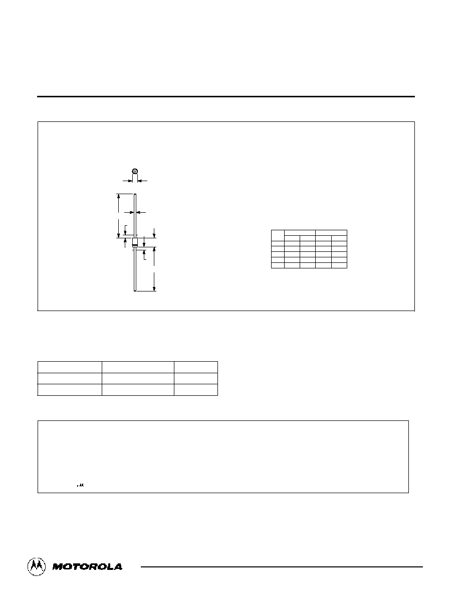
13 Watt DO-41 Surmetic 30
MULTIPLE PACKAGE QUANTITY (MPQ)
REQUIREMENTS
Zener Voltage Regulator Diodes -- Axial Leaded
CASE 59-03
DO-41
PLASTIC
(Refer to Section 10 for Surface Mount, Thermal Data and Footprint Information.)
(Refer to Section 10 for more information on Packaging Specifications.)
Package Option
Tape and Reel
6K
Type No. Suffix
RL
MPQ (Units)
Tape and Ammo
TA
4K
NOTES:
1. ALL RULES AND NOTES ASSOCIATED WITH
JEDEC DO-41 OUTLINE SHALL APPLY.
2. POLARITY DENOTED BY CATHODE BAND.
3. LEAD DIAMETER NOT CONTROLLED WITHIN F
DIMENSION.
K
K
F
A
F
D
MIN
MIN
MAX
MAX
MILLIMETERS
INCHES
DIM
4.07
2.04
0.71
--
27.94
5.20
2.71
0.86
1.27
--
0.160
0.080
0.028
--
1.100
0.205
0.107
0.034
0.050
--
A
B
D
F
K
B
Motorola reserves the right to make changes without further notice to any products herein. Motorola makes no warranty, representation or guarantee regarding
the suitability of its products for any particular purpose, nor does Motorola assume any liability arising out of the application or use of any product or circuit,
and specifically disclaims any and all liability, including without limitation consequential or incidental damages. "Typical" parameters can and do vary in different
applications. All operating parameters, including "Typicals" must be validated for each customer application by customer's technical experts. Motorola does
not convey any license under its patent rights nor the rights of others. Motorola products are not designed, intended, or authorized for use as components in
systems intended for surgical implant into the body, or other applications intended to support or sustain life, or for any other application in which the failure of
the Motorola product could create a situation where personal injury or death may occur. Should Buyer purchase or use Motorola products for any such
unintended or unauthorized application, Buyer shall indemnify and hold Motorola and its officers, employees, subsidiaries, affiliates, and distributors harmless
against all claims, costs, damages, and expenses, and reasonable attorney fees arising out of, directly or indirectly, any claim of personal injury or death
associated with such unintended or unauthorized use, even if such claim alleges that Motorola was negligent regarding the design or manufacture of the part.
Motorola and
are registered trademarks of Motorola, Inc. Motorola, Inc. is an Equal Opportunity/Affirmative Action Employer.
Literature Distribution Centers:
USA: Motorola Literature Distribution; P.O. Box 20912; Phoenix, Arizona 85036.
EUROPE: Motorola Ltd.; European Literature Centre; 88 Tanners Drive, Blakelands, Milton Keynes, MK14 5BP, England.
JAPAN: Nippon Motorola Ltd.; 4-32-1, Nishi-Gotanda, Shinagawa-ku, Tokyo 141, Japan.
ASIA PACIFIC: Motorola Semiconductors H.K. Ltd.; Silicon Harbour Center, No. 2 Dai King Street, Tai Po Industrial Estate, Tai Po, N.T., Hong Kong.