 | –≠–ª–µ–∫—Ç—Ä–æ–Ω–Ω—ã–π –∫–æ–º–ø–æ–Ω–µ–Ω—Ç: 1N821 | –°–∫–∞—á–∞—Ç—å:  PDF PDF  ZIP ZIP |
MOTOROLA
SEMICONDUCTOR
TECHNICAL DATA
Motorola TVS/Zener Device Data
8-159
6.2 Volt OTC 400 mW DO-35 Data Sheet
Temperature-Compensated
Zener Reference Diodes
Temperature-compensated zener reference diodes utilizing a single chip oxide passi-
vated junction for long-term voltage stability. A rugged, glass-enclosed, hermetically sealed
structure.
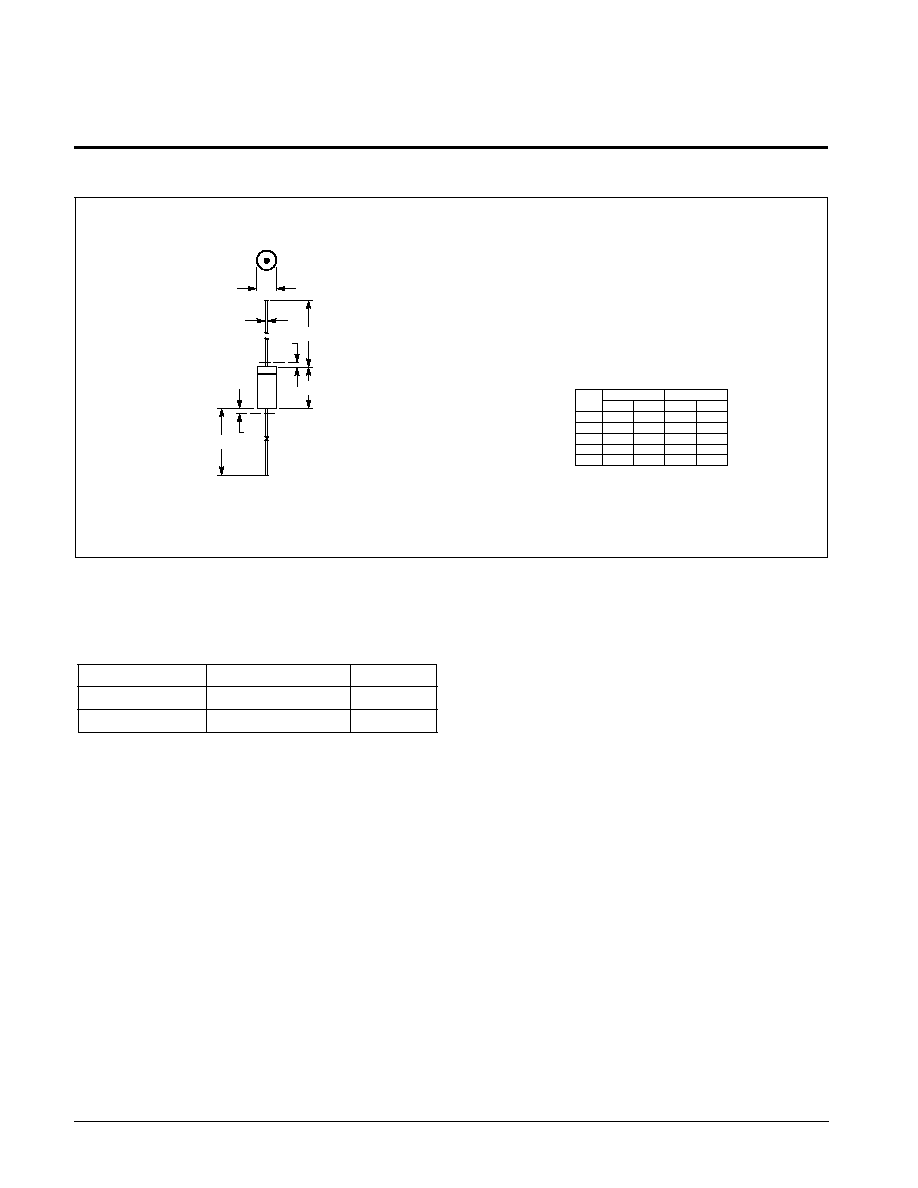
Mechanical Characteristics:
CASE: Hermetically sealed, all-glass
DIMENSIONS: See outline drawing.
FINISH: All external surfaces are corrosion resistant and leads are readily solderable.
POLARITY: Cathode indicated by polarity band.
WEIGHT: 0.2 Gram (approx.)
MOUNTING POSITION: Any
Maximum Ratings
Junction Temperature: ≠ 55 to +175
∞
C
Storage Temperature: ≠ 65 to +175
∞
C
DC Power Dissipation: 400 mW @ TA = 50
∞
C
WAFER FAB LOCATION: Phoenix, Arizona
ASSEMBLY/TEST LOCATION: Phoenix, Arizona
ELECTRICAL CHARACTERISTICS
(TA = 25
∞
C unless otherwise noted. VZ = 6.2 V
±
5%* @ IZT = 7.5 mA) (Note 5)
JEDEC
Type No.
Maximum
Voltage Change
VZ (Volts)
(Note 1)
Ambient
Test Temperature
∞
C
±
1
∞
C
Temperature
Coefficient
For Reference Only
%/
∞
C
(Note 1)
Maximum
Dynamic Impedance
ZZT Ohms
(Note 2)
1N821
0.096
≠ 55, 0, +25, +75, +100
0.01
15
1N823
0.048
0.005
1N825
0.019
0.002
1N827
0.009
0.001
1N829
0.005
0.0005
1N821A
0.096
0.01
10
1N823A
0.048
0.005
1N825A
0.019
0.002
1N827A
0.009
0.001
1N829A
0.005
0.0005
*Tighter-tolerance units available on special request.
1N821,A
1N823,A
1N825,A
1N827,A
1N829,A
TEMPERATURE-
COMPENSATED
SILICON ZENER
REFERENCE DIODES
6.2 V, 400 mW
CASE 299
DO-204AH
GLASS
1N821,A
1N823,A
1N825,A
1N827,A
1N829,A
Motorola TVS/Zener Device Data
8-160
6.2 Volt OTC 400 mW DO-35 Data Sheet
Devices listed in bold, italic are Motorola preferred devices.
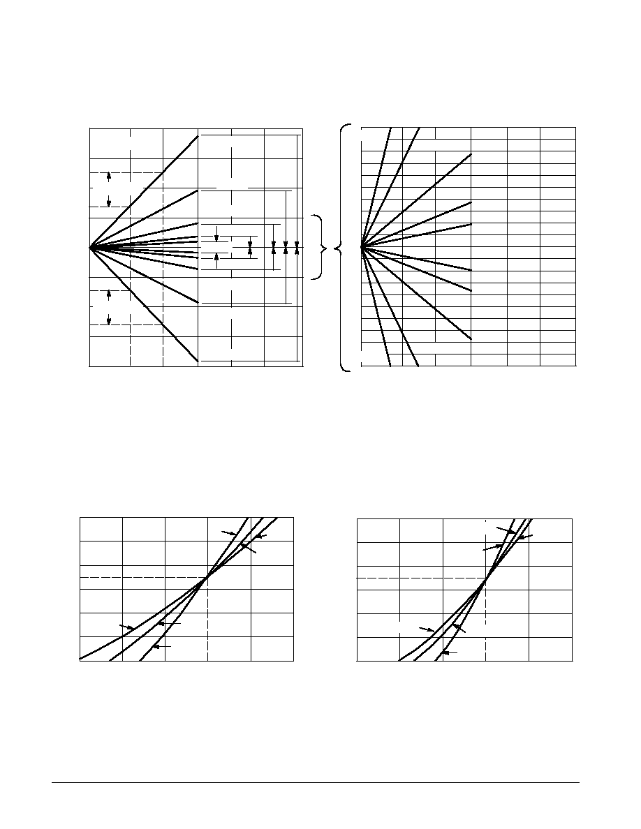
MAXIMUM VOLTAGE CHANGE versus AMBIENT TEMPERATURE
(with IZT = 7.5 mA
±
0.01 mA) (See Note 3)
1N821 through 1N829
Figure 1a
Figure 1b
VZ = +31 mV
VZ = ≠31 mV
IZT = 7.5 mA
1N821,A
1N823,A
1N825,A
1N829,A
1N827,A
1N827,A
1N825,A
1N823,A
1N821,A
100
75
50
25
0
≠25
≠50
≠75
≠10
0≠55
0
50
100
TA, AMBIENT TEMPERATURE (
∞
C)
≠55
0
50
100
≠20
≠15
≠10
≠5
0
5
10
15
20
1N821,A
25
1N823,A
1N825,A
1N827,A
1N829,A
1N829,A
1N827,A
1N825,A
1N823,A
1N821,A
≠25
ZENER CURRENT versus MAXIMUM VOLTAGE CHANGE
(At Specified Temperatures)
(See Note 4)
MORE THAN 95% OF THE UNITS ARE IN THE RANGES INDICATED BY THE CURVES.
Figure 2. 1N821 Series
Figure 3. 1N821A Series
V
Z
, MAXIMUM VOL
T
AGE CHANGE (mV)
(Referenced to ≠55
∞
C)
I Z
, ZENER CURRENT
(mA)
I Z
, ZENER CURRENT
(mA)
10
9
8
7.5
7
6
5
4
≠75
≠50
≠25
0
25
50
+100
∞
C
IZT
+25
∞
C
≠55
∞
C
+25
∞
C
+100
∞
C
≠55
∞
C
10
9
8
7.5
7
6
5
4
VZ, MAXIMUM VOLTAGE CHANGE (mV)
(Referenced to IZT = 7.5 mA)
≠75
≠50
≠25
0
25
50
VZ, MAXIMUM VOLTAGE CHANGE (mV)
(Referenced to IZT = 7.5 mA)
≠55
∞
C
+25
∞
C
+100
∞
C
IZT
≠55
∞
C
+25
∞
C
+100
∞
C
1N821,A
1N823,A
1N825,A
1N827,A
1N829,A
Motorola TVS/Zener Device Data
8-161
6.2 Volt OTC 400 mW DO-35 Data Sheet
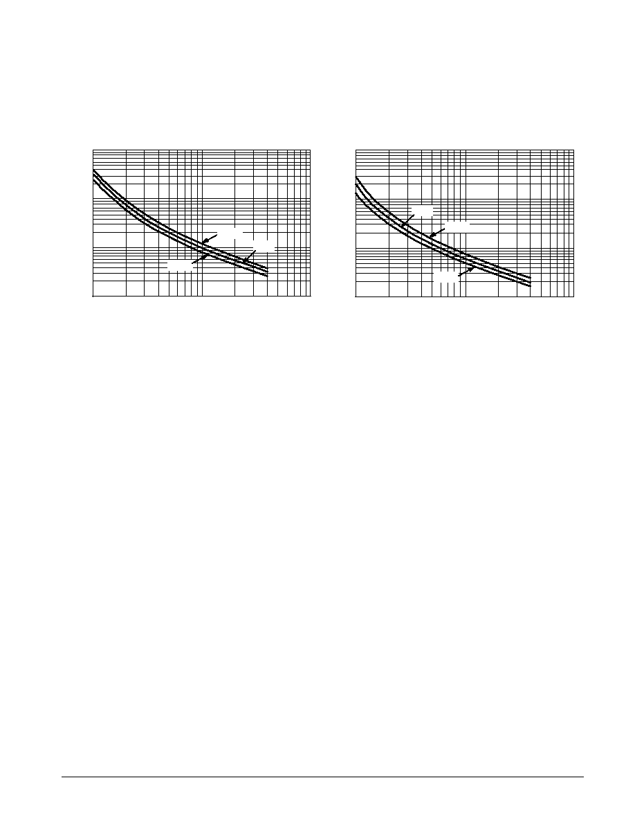
MAXIMUM ZENER IMPEDANCE versus ZENER CURRENT
(See Note 2)
MORE THAN 95% OF THE UNITS ARE IN THE RANGES INDICATED BY THE CURVES.
Figure 4. 1N821 Series
Figure 5. 1N821A Series
1000
1
2
4
6
8
10
20
40
60
80
100
200
400
600
800
Z
Z
, MAXIMUM ZENER IMPEDANCE (OHMS)
Z
Z
, MAXIMUM ZENER IMPEDANCE (OHMS)
1000
1
2
4
6
8
10
20
40
60
80
100
200
400
600
800
IZ, ZENER CURRENT (mA)
1
2
4
6
8 10
20
40
60 80 100
IZ, ZENER CURRENT (mA)
1
2
4
6
8 10
20
40
60 80 100
≠55
∞
C
25
∞
C
100
∞
C
25
∞
C
100
∞
C
≠55
∞
C
NOTE 1. VOLTAGE VARIATION (
VZ) AND TEMPERATURE COEFFICIENT
All reference diodes are characterized by the "box method." This guarantees a maximum volt-
age variation (
VZ) over the specified temperature range, at the specified test current (IZT),
verified by tests at indicated temperature points within the range. VZ is measured and re-
corded at each temperature specified. The
VZ between the highest and lowest values must
not exceed the maximum
VZ given. This method of indicating voltage stability is now used
for JEDEC registration as well as for military qualification. The former method of indicating
voltage stability -- by means of temperature coefficient accurately reflects the voltage devi-
ation at the temperature extremes, but is not necessarily accurate within the temperature
range because reference diodes have a nonlinear temperature relationship. The temperature
coefficient, therefore, is given only as a reference.
NOTE 2.
The dynamic zener impedance, ZZT, is derived from the 60 Hz ac voltage drop which results
when an ac current with an rms value equal to 10% of the dc zener current, IZT, is superim-
posed on IZT. Curves showing the variation of zener impedance with zener current for each
series are given in Figures 4 and 5.
NOTE 3.
These graphs can be used to determine the maximum voltage change of any device in the
series over any specific temperature range. For example, a temperature change from 0 to
+50
∞
C will cause a voltage change no greater than +31 mV or ≠ 31 mV for 1N821 or 1N821A,
as illustrated by the dashed lines in Figure 1. The boundaries given are maximum values. For
greater resolution, an expanded view of the center area in Figure 1a is shown in Figure 1b.
NOTE 4.
The maximum voltage change,
VZ, Figures 2 and 3 is due entirely to the impedance of the
device. If both temperature and IZT are varied, then the total voltage change may be obtained
by graphically adding
VZ in Figure 2 or 3 to the
VZ in Figure 1 for the device under consider-
ation. If the device is to be operated at some stable current other than the specified test cur-
rent, a new set of characteristics may be plotted by superimposing the data in Figure 2 or 3
on Figure 1. For a more detailed explanation see application note in later section.
NOTE 5.
Zener voltage limits at 25
∞
C measured with the test current (IZT) applied with the device junc-
tion in thermal equilibrium at an ambient temperature of 25
∞
C.
Motorola TVS/Zener Device Data
8-162
6.2 Volt OTC 400 mW DO-35 Data Sheet
6.2 Volt OTC 400 mW DO-35
Zener Voltage Reference Diodes
CASE 299-02
DO-204AH
GLASS
(Refer to Section 10 for Surface Mount, Thermal Data and Footprint Information.)
(Refer to Section 10 for more information on Packaging Specifications.)
MULTIPLE PACKAGE QUANTITY (MPQ)
REQUIREMENTS
Package Option
Tape and Reel
5K
Type No. Suffix
RL, RL2(1)
MPQ (Units)
Tape and Ammo
TA, TA2(1)
5K
NOTE: 1. The "2" suffix designates 26 mm tape spacing.
MIN
MIN
MAX
MAX
MILLIMETERS
INCHES
DIM
3.05
1.52
0.46
--
25.40
5.08
2.29
0.56
1.27
38.10
0.120
0.060
0.018
--
1.000
0.200
0.090
0.022
0.050
1.500
A
B
D
F
K
All JEDEC dimensions and notes apply.
NOTES:
1. PACKAGE CONTOUR OPTIONAL WITHIN A AND B
HEAT SLUGS, IF ANY, SHALL BE INCLUDED
WITHIN THIS CYLINDER, BUT NOT SUBJECT TO
THE MINIMUM LIMIT OF B.
2. LEAD DIAMETER NOT CONTROLLED IN ZONE F
TO ALLOW FOR FLASH, LEAD FINISH BUILDUP
AND MINOR IRREGULARITIES OTHER THAN
HEAT SLUGS.
3. POLARITY DENOTED BY CATHODE BAND.
4. DIMENSIONING AND TOLERANCING PER ANSI
Y14.5M, 1982.
B
A
K
D
F
F
K