 | –≠–ª–µ–∫—Ç—Ä–æ–Ω–Ω—ã–π –∫–æ–º–ø–æ–Ω–µ–Ω—Ç: 2N4037 | –°–∫–∞—á–∞—Ç—å:  PDF PDF  ZIP ZIP |

1
Motorola Small≠Signal Transistors, FETs and Diodes Device Data
General Purpose Transistors
PNP Silicon
MAXIMUM RATINGS
Rating
Symbol
2N4036
2N4037
Unit
Collector ≠ Emitter Voltage
VCEO
≠ 65
≠ 40
Vdc
Collector ≠ Base Voltage
VCBO
≠ 90
≠ 60
Vdc
Emitter ≠ Base Voltage
VEBO
≠ 7.0
≠ 7.0
Vdc
Base Current
IB
≠ 0.5
Adc
Collector Current -- Continuous
IC
≠ 1.0
Adc
Continuous Power Dissipation
at or Below TC = 25
∞
C
Linear Derating Factor
PD
5.0
28.6
5.0
28.6
Watts
mW/
∞
C
Continuous Power Dissipation
at or Below TA = 25
∞
C
Linear Derating Factor
PD
1.0
5.72
1.0
5.72
Watts
mW/
∞
C
Operating and Storage Junction
Temperature Range
TJ, Tstg
≠ 65 to +200
∞
C
Lead Temperature
1/16
from Case for 10 Seconds
TL
230
∞
C
THERMAL CHARACTERISTICS
Characteristic
Symbol
2N4036
2N4037
Unit
Thermal Resistance, Junction to Case
R
q
JC
35
35
∞
C/W
ELECTRICAL CHARACTERISTICS
(TA = 25
∞
C unless otherwise noted)
Characteristic
Symbol
Min
Max
Unit
OFF CHARACTERISTICS
Collector ≠ Emitter Sustaining Voltage(1)
(IC = ≠ 100 mAdc, IB = 0)
2N4036
2N4037
VCEO(sus)
≠ 65
≠ 40
--
--
Vdc
Collector ≠ Base Breakdown Voltage
(IC = ≠ 0.1 mAdc)
2N4037
V(BR)CBO
≠ 60
--
Vdc
Collector Cutoff Current
(VCE = ≠ 85 Vdc, VEB = ≠ 1.5 Vdc)
2N4036
(VCE = ≠ 30 Vdc, VEB = ≠ 1.5 Vdc, TC = 150
∞
C)
2N4037
ICEX
--
--
≠ 0.1
≠ 100
mAdc
Collector Cutoff Current
(VCB = ≠ 90 Vdc, IE = 0)
2N4036
(VCB = ≠ 60 Vdc, IE = 0)
2N4037
ICBO
--
--
≠ 1.0
≠ 0.25
µ
Adc
Emitter Cutoff Current
(VEB = ≠ 7.0 Vdc, IC = 0)
2N4036
(VEB = ≠ 5.0 Vdc, IC = 0)
2N4037
IEBO
--
--
≠ 10
≠ 1.0
µ
Adc
1. Pulse Test: Pulse Width
v
300
m
s, Duty Cycle
v
2.0%.
Order this document
by 2N4036/D
MOTOROLA
SEMICONDUCTOR TECHNICAL DATA
2N4036
2N4037
CASE 79≠04, STYLE 1
TO≠39 (TO≠205AD)
1
2
3
©
Motorola, Inc. 1997
COLLECTOR
3
2
BASE
1
EMITTER

2N4036 2N4037
2
Motorola Small≠Signal Transistors, FETs and Diodes Device Data
ELECTRICAL CHARACTERISTICS
(TA = 25
∞
C unless otherwise noted) (Continued)
Characteristic
Symbol
Min
Max
Unit
ON CHARACTERISTICS
DC Current Gain
(IC = ≠ 0.1 mAdc, VCE = ≠10 Vdc)
2N4036
(IC = ≠1.0 mAdc, VCE = ≠10 Vdc)
2N4037
(IC = ≠150 mAdc, VCE = ≠10 Vdc)(1)
2N4036
2N4037
(IC = ≠150 mAdc, VCE = ≠ 2.0 Vdc)(1)
2N4036
(IC = ≠ 500 mAdc, VCE = ≠10 Vdc)(1)
2N4036
hFE
20
15
40
50
20
20
--
--
140
250
200
--
--
Collector ≠ Emitter Saturation Voltage(1)
2N4036
(IC = ≠ 150 mAdc, IB = ≠ 15 mAdc)
2N4037
VCE(sat)
--
--
≠ 0.65
≠ 1.4
Vdc
Base ≠ Emitter Saturation Voltage(1)
(IC = ≠ 150 mAdc, IB = ≠ 15 mAdc)
2N4036
VBE(sat)
--
≠1.4
Vdc
Base ≠ Emitter On Voltage(1)
(IC = ≠ 150 mAdc, VCE = ≠ 10 Vdc)
2N4037
VBE(on)
--
≠ 1.5
Vdc
SMALL≠ SIGNAL CHARACTERISTICS
Collector≠Base Capacitance
(VCB = ≠ 10 Vdc, f = 1.0 MHz)
2N4037
Ccb
--
30
pF
Current Gain -- High Frequency
2N4036
(IC = ≠ 50 mAdc, VCE = ≠ 10 Vdc, f = 20 MHz)
2N4037
|hfe|
3.0
3.0
--
10
--
SWITCHING CHARACTERISTICS
Rise Time
(IB1 = ≠ 15 mAdc)
2N4036
tr
--
70
ns
Storage Time
(IB2 = ≠ 15 mAdc)
2N4036
ts
--
600
ns
Fall Time
(IB2 = ≠ 15 mAdc)
2N4036
tf
--
100
ns
Turn≠On Time
(IB1 = IB2)
2N4036
ton
--
110
ns
Turn≠Off Time
(IB1 = IB2)
2N4036
toff
--
700
ns
1. Pulse Test: Pulse Width
v
300
m
s, Duty Cycle
v
2.0%.
2N4036 2N4037
3
Motorola Small≠Signal Transistors, FETs and Diodes Device Data
300
µ
s
500
µ
s
1.0 ms
50
µ
s
100
µ
s
DC OPERATION
PULSED OPERATION*
9.3
5.0
3.0
2.0
1.0
7.0
h
FE
, NORMALIZED DC CURRENT
GAIN
P
T
, MAXIMUM
TRANSIST
OR
DISSIP
A
TION (W)
I CBO
, COLLECT
OR CUT
OFF CURRENT
(mA)
I C
, COLLECT
OR
CURRENT
(mA)
h
FE
, SMALL≠SIGNAL
FOR
W
ARD
CURRENT
TRANSFER RA
TIO
I C
, COLLECT
OR
CURRENT
(A)
≠ 0.1
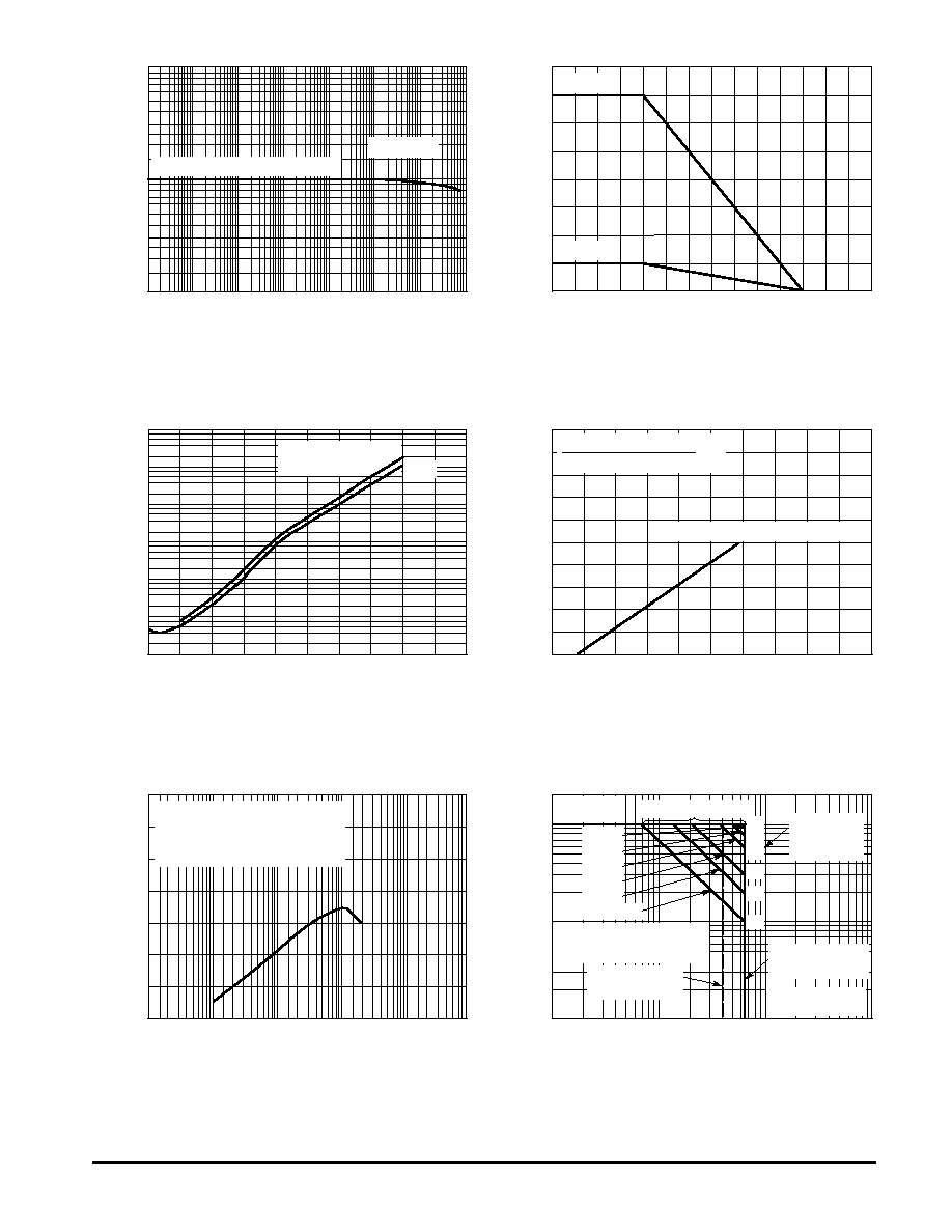
Figure 1. Current Gain Characteristics versus
Collector≠Emitter Voltage
IC, COLLECTOR CURRENT (mA)
≠ 75
Figure 2. Dissipation Derating Curve
CASE OR AMBIENT TEMPERATURE (TC OR TA) ≠
∞
C
10
7.0
200
TJ, JUNCTION TEMPERATURE (
∞
C)
≠ 0.5
VCE(sat), COLLECTOR≠TO≠EMITTER SATURATION VOLTAGE (V)
≠10≠ 5
≠ 400
Figure 3. Typical Collector≠Cutoff Current
versus Junction Temperature
Figure 4. Typical Saturation≠Voltage
Characteristics
≠ 100
IC, COLLECTOR CURRENT (mA)
≠ 100
VCE, COLLECTOR≠TO≠EMITTER VOLTAGE (V)
8.0
≠ 0.01
Figure 5. Typical Small≠Signal Beta
Characteristics
Figure 6. Maximum Safe Operating Areas
(SOA)
1.0
0.1
≠ 1.0
≠ 10
≠ 100
VCE = ≠ 10 V
AMBIENT TEMPERATURE (TA) = 25
∞
C
(AT TA)
(AT TC)
6.0
5.0
4.0
3.0
2.0
1.0
0
≠ 25 0
50
100
150
200
≠10≠ 6
≠10≠ 7
≠10≠ 8
≠10≠ 9
≠10≠10
175
150
125
100
75
50
25
0
COLLECTOR≠TO≠BASE
VOLTAGE ≠ 40 V
≠ 20 V
≠ 600
≠ 200
0
≠ 0.15
≠ 0.25
≠ 0.35
AMBIENT TEMPERATURE (TA) = 25
∞
C
COLLECTOR CURRENT (IC) = 10
BASE CURRENT (IB)
≠ 1000
≠ 10
≠ 1.0
10
6.0
4.0
2.0
0
COLLECTOR≠TO≠EMITTER VOLTAGE
(VCE) = ≠10 V
FREQUENCY = 20 MHz
AMBIENT TEMPERATURE (TA) = 25
∞
C
CASE TEMPERATURE (TC) = 25
∞
C
(CURVES MUST BE DERATED LINEARLY
WITH INCREASE OF TEMPERATURE)
VCEO MAX = 40 V
(2N4037)
VCEO MAX = ≠ 65 V
(2N4036)
*FOR SINGLE
NONREPETITIVE PULSE
≠ 0.1
1.0
≠ 10
≠ 1.0
IC MAX.
(CONTINUOUS)
NORMALIZED
POWER
MULTIPLIER

2N4036 2N4037
4
Motorola Small≠Signal Transistors, FETs and Diodes Device Data
PACKAGE DIMENSIONS
CASE 079≠04
(TO≠205AD)
ISSUE N
NOTES:
1. DIMENSIONING AND TOLERANCING PER ANSI
Y14.5M, 1982.
2. CONTROLLING DIMENSION: INCH.
3. DIMENSION J MEASURED FROM DIMENSION A
MAXIMUM.
4. DIMENSION B SHALL NOT VARY MORE THAN
0.25 (0.010) IN ZONE R. THIS ZONE
CONTROLLED FOR AUTOMATIC HANDLING.
5. DIMENSION F APPLIES BETWEEN DIMENSION
P AND L. DIMENSION D APPLIES BETWEEN
DIMENSION L AND K MINIMUM. LEAD
DIAMETER IS UNCONTROLLED IN DIMENSION
P AND BEYOND DIMENSION K MINIMUM.
STYLE 1:
PIN 1. EMITTER
2. BASE
3. COLLECTOR
SEATING
PLANE
R
E
F
B
C
K
L
P
D
3 PL
≠T≠
≠A≠
≠H≠
M
J
G
2
3
1
DIM
MIN
MAX
MIN
MAX
MILLIMETERS
INCHES
A
0.335
0.370
8.51
9.39
B
0.305
0.335
7.75
8.50
C
0.240
0.260
6.10
6.60
D
0.016
0.021
0.41
0.53
E
0.009
0.041
0.23
1.04
F
0.016
0.019
0.41
0.48
G
0.200 BSC
5.08 BSC
H
0.028
0.034
0.72
0.86
J
0.029
0.045
0.74
1.14
K
0.500
0.750
12.70
19.05
L
0.250
≠≠≠
6.35
≠≠≠
M
45 BSC
45 BSC
P
≠≠≠
0.050
≠≠≠
1.27
R
0.100
≠≠≠
2.54
≠≠≠
_
_
M
A
M
0.36 (0.014)
H
M
T
Motorola reserves the right to make changes without further notice to any products herein. Motorola makes no warranty, representation or guarantee regarding
the suitability of its products for any particular purpose, nor does Motorola assume any liability arising out of the application or use of any product or circuit, and
specifically disclaims any and all liability, including without limitation consequential or incidental damages. "Typical" parameters which may be provided in Motorola
data sheets and/or specifications can and do vary in different applications and actual performance may vary over time. All operating parameters, including "Typicals"
must be validated for each customer application by customer's technical experts. Motorola does not convey any license under its patent rights nor the rights of
others. Motorola products are not designed, intended, or authorized for use as components in systems intended for surgical implant into the body, or other
applications intended to support or sustain life, or for any other application in which the failure of the Motorola product could create a situation where personal injury
or death may occur. Should Buyer purchase or use Motorola products for any such unintended or unauthorized application, Buyer shall indemnify and hold Motorola
and its officers, employees, subsidiaries, affiliates, and distributors harmless against all claims, costs, damages, and expenses, and reasonable attorney fees
arising out of, directly or indirectly, any claim of personal injury or death associated with such unintended or unauthorized use, even if such claim alleges that
Motorola was negligent regarding the design or manufacture of the part. Motorola and are registered trademarks of Motorola, Inc. Motorola, Inc. is an Equal
Opportunity/Affirmative Action Employer.
Mfax is a trademark of Motorola, Inc.
How to reach us:
USA / EUROPE / Locations Not Listed: Motorola Literature Distribution;
JAPAN: Nippon Motorola Ltd.; Tatsumi≠SPD≠JLDC, 6F Seibu≠Butsuryu≠Center,
P.O. Box 5405, Denver, Colorado 80217. 303≠675≠2140 or 1≠800≠441≠2447
3≠14≠2 Tatsumi Koto≠Ku, Tokyo 135, Japan. 81≠3≠3521≠8315
Mfax
TM
: RMFAX0@email.sps.mot.com ≠ TOUCHTONE 602≠244≠6609
ASIA/PACIFIC: Motorola Semiconductors H.K. Ltd.; 8B Tai Ping Industrial Park,
INTERNET: http://Design≠NET.com
51 Ting Kok Road, Tai Po, N.T., Hong Kong. 852≠26629298
2N4036/D